

Etching method and method for manufacturing semiconductor device
- Summary
- Abstract
- Description
- Claims
- Application Information
AI Technical Summary
Benefits of technology
Problems solved by technology
Method used
Image

Examples
embodiment 1
[0061]In this embodiment, a method for etching that is one embodiment of the present invention will be described.
[0062]In one embodiment of the method for etching described in this embodiment, part of a stacked semiconductor film in which an amorphous semiconductor film is provided on a crystalline semiconductor film is etched using a mixed gas including at least a Br-based gas, a F-based gas, and an oxygen gas, so that part of the crystalline semiconductor film in the stacked semiconductor film is exposed.
[0063]In one embodiment of the method for etching described in this embodiment, an etching mask is formed over a first region in a stacked semiconductor film in which an amorphous semiconductor film is provided on a crystalline semiconductor film and whose top surface includes the first region and a second region; and part of the crystalline semiconductor film in the second region is exposed by etching with the use of a mixed gas including at least a Br-based gas, a F-based gas, a...
embodiment 2
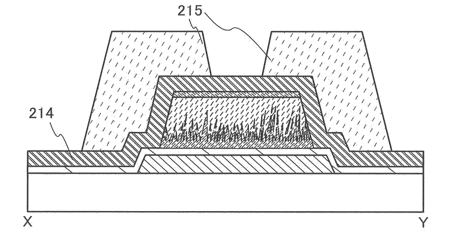
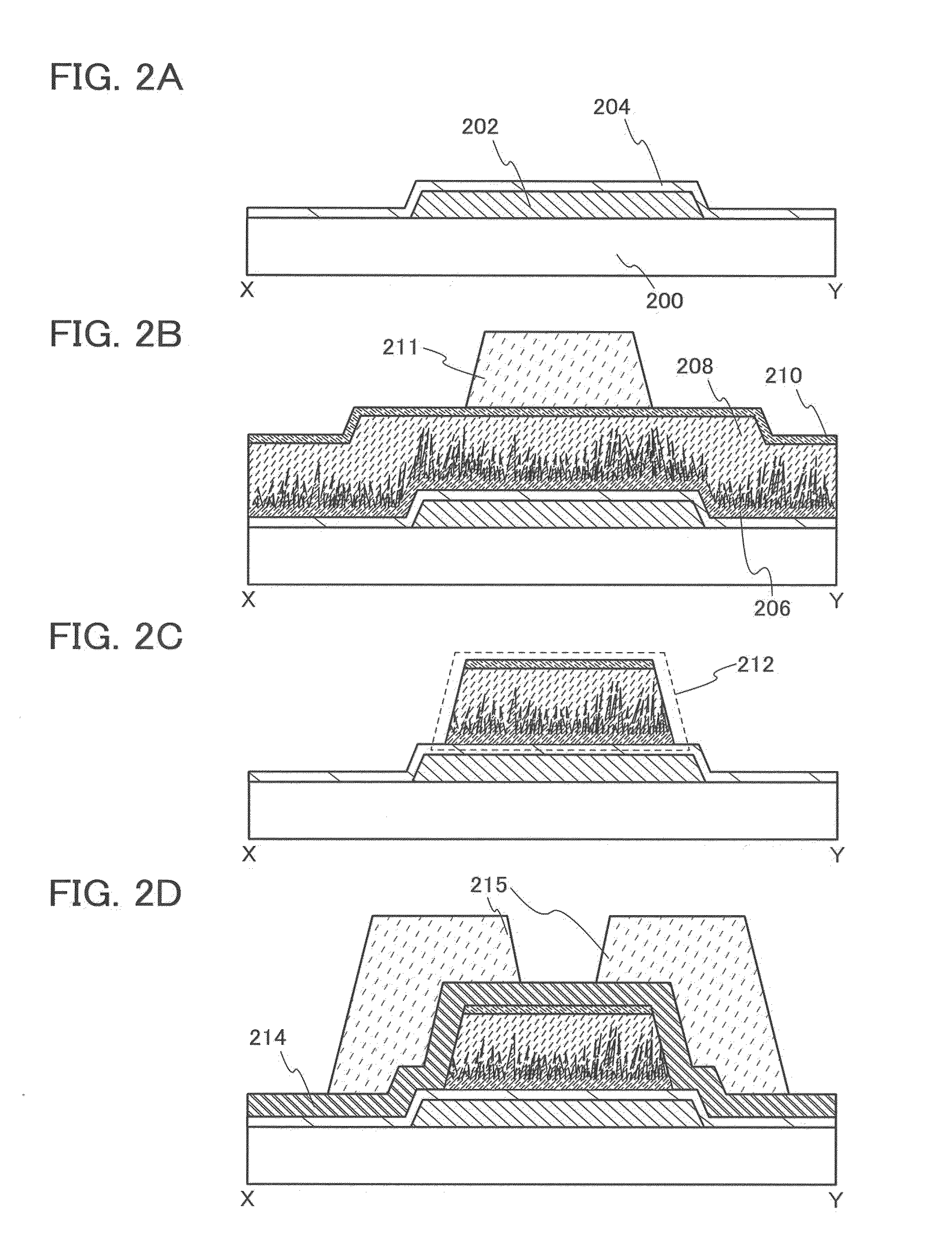
[0081]In this embodiment, a manufacturing method of a semiconductor device that is one embodiment of the present invention will be described. Specifically, a method for manufacturing a thin film transistor to which the method for etching described in Embodiment 1 is applied will be described with reference to FIGS. 2A to 2D and FIGS. 3A to 3D.
[0082]First, a first conductive layer 202 is formed over a substrate 200, and a first insulating layer 204 is formed so as to cover the first conductive layer 202 (FIG. 2A).
[0083]The substrate 200 is an insulating substrate. As the substrate 200, for example, in addition to a glass substrate, a quartz substrate, and a ceramic substrate, a plastic substrate or the like with heat resistance that is high enough to withstand a process temperature in this manufacturing process can be used. In the case where the substrate 200 is a glass substrate, any of the substrate of the first generation (e.g., 320 mm×400 mm) to the tenth generation (e.g., 2950 m...
embodiment 3
[0132]In this embodiment, a semiconductor device that is one embodiment of the present invention will be described with reference to the drawings.
[0133]In a thin-film transistor of this embodiment, an “additional gate electrode (hereinafter also referred to as a second gate electrode)” is provided on the side opposite to a gate electrode (hereinafter also referred to as a first gate electrode) and a channel formation region is increased by the additional gate electrode. Thus, an additional gate electrode is provided, on-state current can be increased.
[0134]FIGS. 4A, 4B, and 4C are a cross-sectional view and top views illustrating semiconductor devices that are an embodiment of the present invention. FIG. 4A is a cross sectional view along the line X-Y in the top view of FIG. 4B. The semiconductor device illustrated in FIGS. 4A and 4B includes a first conductive layer 302 provided over a substrate 300, a first insulating layer 304 covering the first conductive layer 302, a first semi...
PUM
 Abstract
Description
Claims
Application Information