Self-learning selection method for optimal parameters of chip module

A chip module and optimal parameter technology, which is applied in the detection of faulty computer hardware, function inspection, etc., can solve problems such as symptom confusion, manual configuration, and time-consuming debugging, and achieve the effect of reducing efficiency and time, and enhancing unity

Pending Publication Date: 2022-04-15
SHANGHAI HUAHONG INTEGRATED CIRCUIT +1
View PDF0 Cites 1 Cited by
  • Summary
  • Abstract
  • Description
  • Claims
  • Application Information

AI Technical Summary

Problems solved by technology

[0003] At present, in the verification process of the existing chip analog modules, the conventional test vectors are tested using design standard values, and it is difficult to achieve better coverage and accurate diagnosis capabilities in the full threshold range for high-precision and complex circuits.
It takes a long time to debug related tests using non-self-learning algorithm libraries, and most of the test items have wrong symptoms, misjudgments and symptoms confusion
At the same time, test scripts and instrument program-controlled incentives are generally not integrated for the entire verification system. Most of the verification work needs to be manually configured, which wastes a lot of labor costs and debugging time, and increases the risk of errors in manual debugging operations. Test Quality and Results

Method used


Image

  • Self-learning selection method for optimal parameters of chip module
  • Self-learning selection method for optimal parameters of chip module
  • Self-learning selection method for optimal parameters of chip module

Examples


Embodiment Construction

[0048] The following is a detailed description of the patent of the present invention in combination with specific software and hardware operation construction as an example:

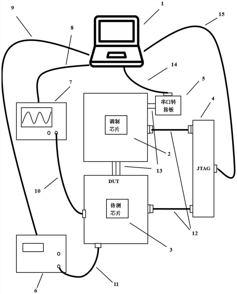
[0049] figure 1 Including 1. PC terminal, 2. On-board chip for modulation, 3. On-board chip for testing, 4. JTAG debugging channel, 5. USB to serial port adapter board, 6. Program-controlled digital power supply, 7. High-precision signal Source, 8. Instrument adapter cable (USB, COM, LAN, GPIB), 9. (same as 8), 10. Coaxial cable, 11. (same as 10), 12. Cable, 13. DuPont line, 14 .USB cable, 15. (same as 14).

[0050] The exemplary embodiments of the present invention will be further described in detail below in conjunction with the accompanying drawings and specific embodiments:

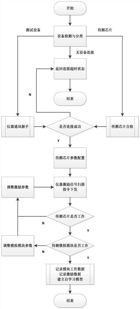
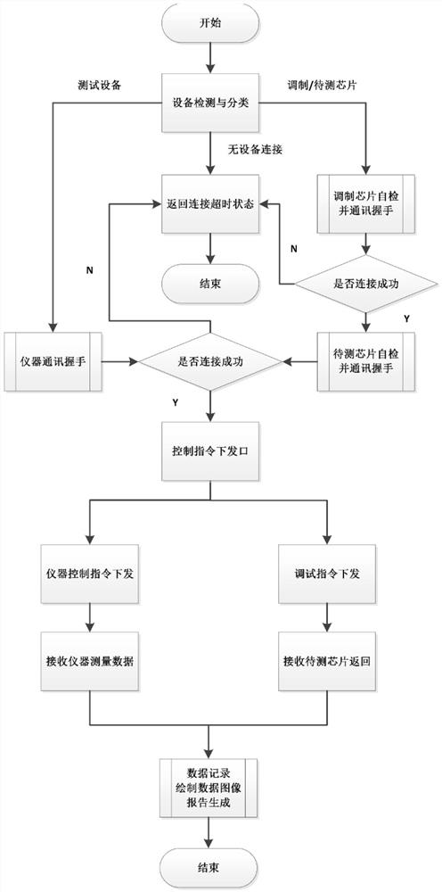
[0051] figure 1 Shown is the overall application structure diagram of the self-learning selection method of the optimal parameter of the chip module of the present invention. The overall testing process is achieved throug...


PUM


Abstract

The invention discloses a self-learning optimization method for optimal parameter selection of a chip module, which is a rapid automatic algorithm and is used for traversing and combining configuration parameters of a chip so as to select a group of external excitation configuration and chip configuration tuning parameters for ensuring the optimal overall performance of the chip. The device is especially suitable for automatic testing of performance verification of a low-power-consumption microcontroller (hereinafter referred to as MCU) chip simulation module sensitive to input simulation parameters and a digital-analog interface module. The method is composed of a data analysis self-learning algorithm and a program control automatic acquisition platform. The data analysis self-learning algorithm adjusts various parameters of the chip to be evaluated through the program-controlled automatic acquisition platform, obtains performance index feedback, obtains working environment ranges of different parameters, and analyzes and obtains optimal parameters after the performance and the working range are balanced; data are updated according to batch chip analysis results, a standard database is established, new chips are selectively scanned according to parameters and a working environment range, the test time is saved, and early warning is provided when a standard curve is deviated.

Description

technical field [0001] The invention relates to a test, control and analysis technology in the technical field of chip verification, in particular to the aspects of performance analysis test and program-controlled test instrument automatic measurement in chip simulation module verification. Background technique [0002] In recent years, with the rapid development of large-scale integrated circuit development and manufacturing technology, various indicators of chip analog modules have become more and more key factors to measure the performance of some unique chips. High integration and complex functions are also the design requirements for such chips Features to meet the needs of different industries. Therefore, while the logical function of the functional module is confirmed, the performance screening and verification of the chip module is a key link after the chip is taped out. Factors such as processing and packaging will cause personality deviation. It is necessary to re...

Claims


Application Information

Patent Timeline
Patent Type & Authority Applications(China)
IPC IPC(8): G06F11/26
Inventor 张瀚文戴昭君
Owner SHANGHAI HUAHONG INTEGRATED CIRCUIT
Why Eureka
Try Eureka