Semiconductor packaging structure and preparation method

A packaging structure and semiconductor technology, applied in semiconductor/solid-state device manufacturing, semiconductor devices, semiconductor/solid-state device components, etc., can solve problems such as high integration density and large transmission bandwidth.

Pending Publication Date: 2022-04-15
NAT CENT FOR ADVANCED PACKAGING +1
View PDF0 Cites 0 Cited by
  • Summary
  • Abstract
  • Description
  • Claims
  • Application Information

AI Technical Summary

Problems solved by technology

[0004] Therefore, the technical problem to be solved by the present invention is to overcome the defect that the existing packaging structure cannot ...

Method used


Image

  • Semiconductor packaging structure and preparation method
  • Semiconductor packaging structure and preparation method
  • Semiconductor packaging structure and preparation method

Examples


Embodiment 1

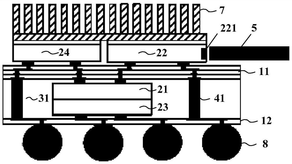
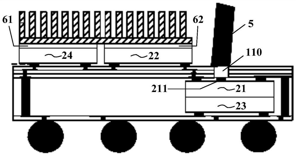
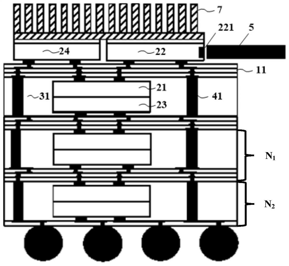
[0050] This embodiment provides a semiconductor packaging structure, such as figure 1 shown, including:

[0051] The second rewiring structure 12; the first functional chip 21 and the pressure supply chip 23 located on the side of the second rewiring structure 12, the pressure supply chip 23 is flip-chip mounted on the side of the second rewiring structure 12, The first functional chip 21 is installed on the side of the pressure supply chip 23 away from the second rewiring structure 12; it is located on the side of the second rewiring structure 12 and covers the side of the first functional chip 21 The wall and the first plastic sealing layer 31 of the side wall of the pressure supply chip 23; the first conductive connection located on the side of the first functional chip 21 and the pressure supply chip 23 and penetrating through the first plastic sealing layer 31 Part 41; the first rewiring structure 11 located on the side of the first plastic encapsulation layer 31 away fr...

Embodiment 2

[0063] This embodiment provides a method for preparing a semiconductor packaging structure, and the schematic flow chart is as follows Figure 5 shown, including the following steps:

[0064] Step S1: forming a second rewiring structure 12;

[0065] Step S2: forming a first conductive connector 41 on one side of the second rewiring structure 12 and electrically connecting with the second rewiring structure 12;

[0066] Step S3: Provide the first functional chip 21 and the pressure supply chip 23, flip-chip the pressure supply chip 23 on the side of the second rewiring structure 12, and mount the first functional chip on the pressure supply chip On the side away from the second rewiring structure, the first conductive connector 41 is located on the side of the first functional chip 21 and the pressure supply chip 23;

[0067] Step S4: Forming a first plastic encapsulation layer 31 on one side of the second rewiring structure 12, the first plastic encapsulation layer 31 covers...


PUM


Abstract

The invention provides a semiconductor packaging structure and a preparation method. The semiconductor package structure includes: a second redistribution structure; the voltage supply chip is inversely arranged on the second rewiring structure, and the first functional chip is positively arranged on one side, deviating from the second rewiring structure, of the voltage supply chip; the first plastic packaging layer is positioned on one side of the second rewiring structure and covers the first functional chip and the voltage supply chip; the first conductive connecting piece is positioned at the side parts of the first functional chip and the voltage supply chip; the first rewiring structure is located on the side, away from the second rewiring structure, of the first plastic packaging layer, the first rewiring structure is electrically connected with the front face of the first functional chip, and the first conductive connecting piece is electrically connected with the first rewiring structure and the second rewiring structure; and the second functional chip is inversely arranged on one side, deviating from the second rewiring structure, of the first rewiring structure and is electrically connected with the first rewiring structure. The semiconductor packaging structure is high in integration density and large in transmission bandwidth.

Description

technical field [0001] The invention relates to the technical field, in particular to a semiconductor packaging structure and a preparation method. Background technique [0002] In application scenarios such as data centers or high-performance computing, communication data rates are developing in the direction of ultra-high throughput and high-quality transmission. Therefore, photoelectric conversion has developed from edge pluggable modules to photoelectric co-packaging (CPO) technology, combining CPO with ASICs such as Switch / FPGA / CPU are integrated on a package substrate. In order to increase the integration density, the size of CPO is getting smaller and smaller. Therefore, it is very important to propose a small CPO packaging structure. In addition, in order to reduce the size of the CPO, the industry advocates placing the power supply chip (PMIC) of the CPO on the package substrate integrated with the Switch, but this will lengthen the power supply path, thereby incre...

Claims


Application Information

Patent Timeline
IPC IPC(8): H01L25/18H01L23/367H01L23/538H01L23/31H01L21/50H01L21/56H01L21/60G02B6/42
CPCH01L2224/18H01L2224/16225H01L2224/73253
Inventor 何慧敏
Owner NAT CENT FOR ADVANCED PACKAGING
Why Eureka
Try Eureka