Memory system and operating method thereof

A technology of memory, memory chips, applied in the field of memory systems, to achieve the effects of easy manufacturing process and shipment control, avoiding restrictions, large margins and durability

Pending Publication Date: 2022-04-22
WINBOND ELECTRONICS CORP
View PDF0 Cites 0 Cited by
  • Summary
  • Abstract
  • Description
  • Claims
  • Application Information

AI Technical Summary

Problems solved by technology

memory array

Method used


Image

  • Memory system and operating method thereof
  • Memory system and operating method thereof
  • Memory system and operating method thereof

Examples


Embodiment Construction

[0023] Reference will now be made in detail to the exemplary embodiments of the present invention, examples of which are illustrated in the accompanying drawings. Wherever possible, the same reference numbers will be used in the drawings and description to refer to the same or like parts.

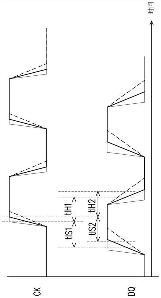
[0024] exist figure 1 In , the thin solid line represents the signal waveform received outside the package structure of the memory system. The thick solid line represents the signal waveform received by the memory chip when there is only one memory chip in the package structure. The dotted line represents the signal waveform received by the memory chip when two memory chips are stacked in the package structure.

[0025] Due to the influence of the input capacitor on the pin, the signal waveform of the thick solid line and the dotted line will have a signal delay compared with the signal waveform of the thin solid line, and the delay of the data signal DQ will be greater than the delay of ...


PUM


Abstract

The invention provides a memory system and an operation method thereof. The memory system comprises a plurality of memory chips which are mutually connected. Each memory chip comprises a memory array, a read-write data strobe pin position, a lookup table memory, a chip number identification circuit and a control logic circuit. The memory array stores data. And the read-write data strobe pin position is connected with the read-write data strobe pin positions of other memory chips. The lookup table memory pre-stores a plurality of fine tuning offset values associated with the chip connection number. The chip number identification circuit identifies the current chip connection number according to the state information and finds out the selected fine tuning offset value from the lookup table memory according to the current chip connection number. The control logic circuit transmits the data signal in response to the clock signal, and adjusts the setting and holding time between the clock signal and the data signal according to the selected fine tuning offset value.

Description

technical field [0001] The present invention relates to a memory system, in particular to a memory system including a plurality of stacked memory chips and an operation method thereof. Background technique [0002] To meet the demand for miniaturization, the packaging structure of the conventional memory system includes a plurality of stacked memory chips to increase the memory density. In the memory system with HyperRAM interface, between multiple memory chips, the CS# pin, CK pin, DQ pin, RWDS pin, and RESET# pin of each memory chip will be the same as those of other memory chips. The bits are connected to each other to share the signal on the pin. Each memory chip can receive a different chip identification signal DIE_STK for corresponding operations. [0003] Since the input capacitance of the CK pin is different from that of the DQ pin, for example, the clock signal on the CK pin and the data signal on the DQ pin can be stored through a non-volatile laser fuse or elec...

Claims


Application Information

Patent Timeline
IPC IPC(8): G11C5/06G11C5/12G11C7/22
CPCG11C5/063G11C5/12G11C7/222H03K19/01742H03K19/17728G11C29/50012G11C29/023G11C29/028G11C2207/2254G11C2029/4402G11C8/12G11C2029/0407G11C7/20G11C7/22G11C7/1006G11C11/4096G11C11/4076G11C11/4093G11C17/143G11C8/18G11C8/06
Inventor 森郁
Owner WINBOND ELECTRONICS CORP
Why Eureka
Try Eureka