Microstrip line-based strip electron beam focusing method, device and application

A strip-shaped electronic and focusing device technology, which is applied in the direction of time-of-flight electron tubes, circuits, discharge tubes, etc., can solve the problems of aggravated focusing difficulty, Diocotron instability, and longer time, so as to achieve good focusing effect and unstoppable suppression. The effect of stability and simple processing

Active Publication Date: 2022-04-29
UNIV OF ELECTRONICS SCI & TECH OF CHINA
View PDF11 Cites 0 Cited by
  • Summary
  • Abstract
  • Description
  • Claims
  • Application Information

AI Technical Summary

Problems solved by technology

In addition, because the operating voltage of the microstrip vacuum electronic device is smaller, the charge density of the electron beam will be higher and the repulsion force will be stronger at the same current density, and, due to the small operating voltage of the microstrip vacuum electronic device, it is also It makes the time for the electron beam to pass through the focusing system longer, which increases the difficulty of focusing the electron beam
Therefore, the strip-shaped electron beam in the microstrip vacuum electronic device is very difficult to be focused by conventional means.
For example, it is found in experiments that the ribbon-shaped electron beam breaks and forms multiple filaments after a certain distance of transmission under the action of a magnetic field along the electron beam transmission direction (z direction), which is called Diocotron instability. or Diocotron instability, which further exacerbates the difficulty of focusing

Method used


Image

  • Microstrip line-based strip electron beam focusing method, device and application
  • Microstrip line-based strip electron beam focusing method, device and application
  • Microstrip line-based strip electron beam focusing method, device and application

Examples


Embodiment 1

[0036] A focusing method of a strip-shaped electron beam based on a microstrip line, comprising: generating an electric field in the space where the microstrip line exists, and the electric field makes the edges of the strip-shaped electron beam of the microstrip line equipotential.

[0037] The invention is based on a stable condition of the focus of the ribbon-shaped electron beam, that is, when the edge of the ribbon-shaped electron beam is equipotential, the ribbon-shaped electron beam can be stably transmitted.

[0038] However, this stable condition is not a conventional technical means for those skilled in the art. This is because, in general, the ribbon-shaped electron beam is focused by a uniform magnetic field, but since the space charge field distribution of the ribbon-shaped electron beam is not axisymmetric, a very high magnetic field is required for focusing.

[0039] In order to study the instability of the ribbon-shaped electron beam in a uniform magnetic field...

Embodiment 2

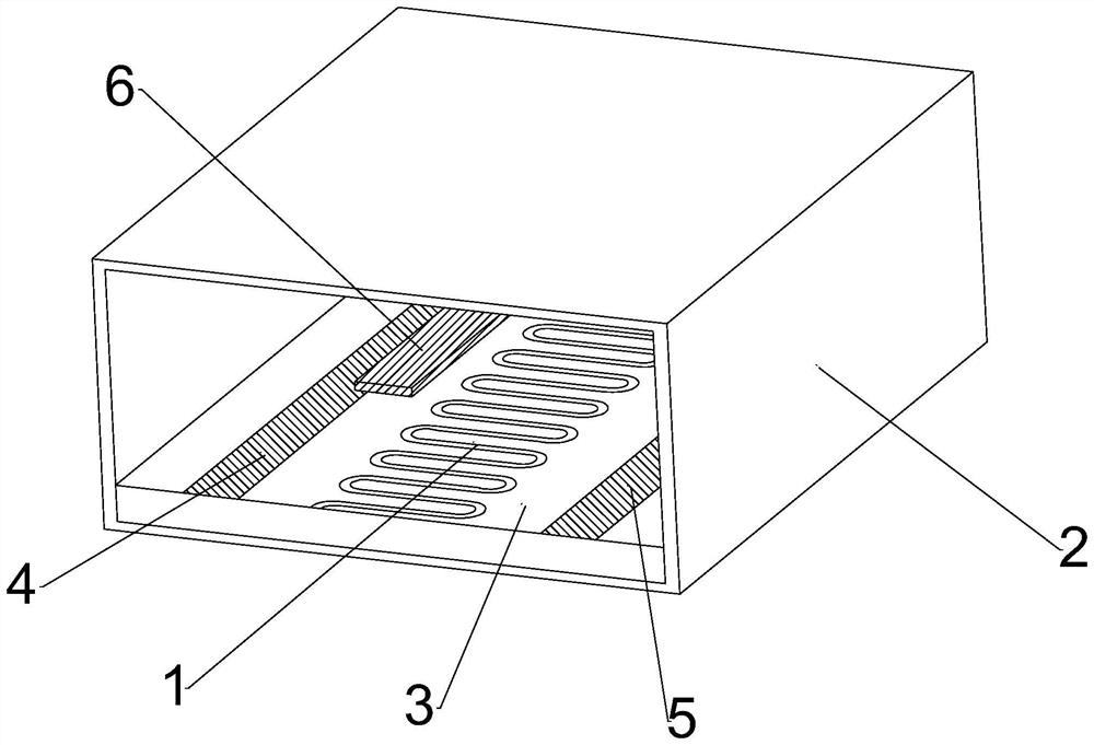
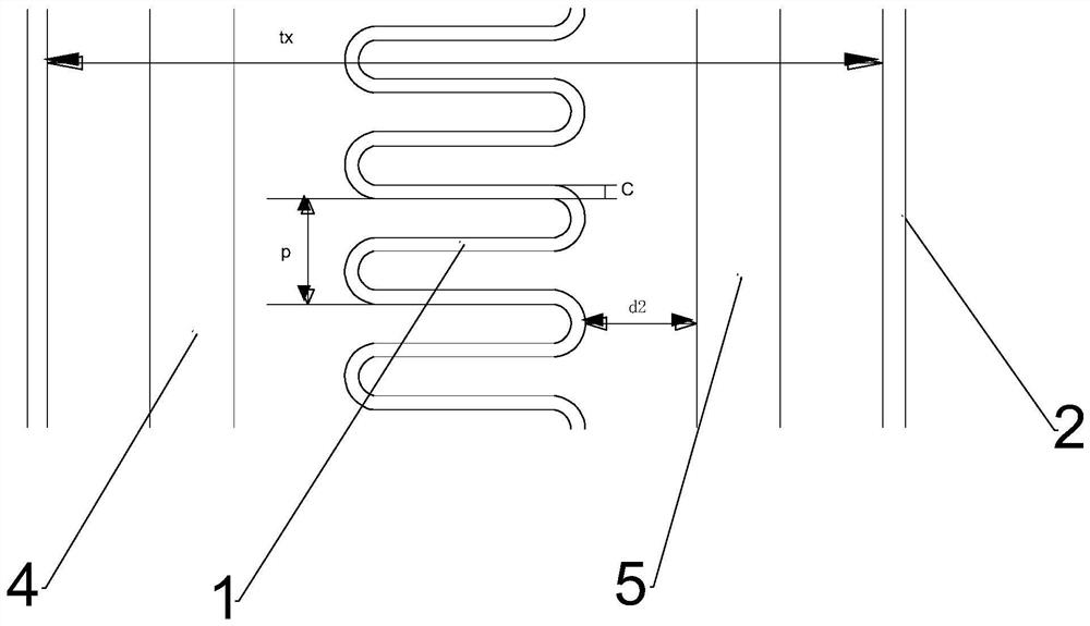
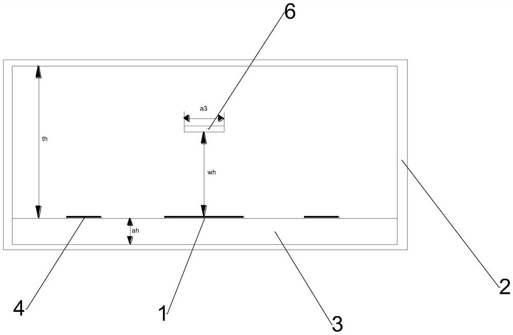
[0046] Such as figure 1 As shown, a focusing device based on a strip-shaped electron beam of a microstrip line is used to implement a focusing method of a strip-shaped electron beam of a microstrip line, including a metal shell 2, a microstrip line 1, a dielectric substrate 3 and several metal wires (4, 5, 6), the length direction of the metal wire is set with the moving direction of the strip-shaped electron beam. In this embodiment, the microstrip line 1 is sinusoidal, and the direction of its periodic extension is the strip-shaped electron beam. The direction of motion, specifically, such as figure 2 As shown, the width of the microstrip line 1 is a, the period length is p, and the line width is c.

[0047] Since the space charge field in the existing microstrip vacuum electronic device does not meet this condition, a number of metal wires are added to the microstrip vacuum electronic device, and then voltage is applied to the channel wall, the metal wire, and the microst...

Embodiment 3

[0057] A kind of application of the strip electron injection based on microstrip line, comprises the steps:

[0058] Apply the above-mentioned focusing device to fields including but not limited to high-resolution radar, high-speed data communication, electronic attack, and radio astronomy;

[0059] The focusing device needs to be debugged before application, and the debugging method is as follows:

[0060] Applying a voltage to both ends of the microstrip line of the focusing device, thereby generating a strip-shaped electron beam;

[0061] An electric field is generated in the space in the metal channel of the focusing device, so that the edges of the strip-shaped electron beam of the microstrip line of the focusing device are equipotential.

[0062] In this embodiment, an electric field is generated in the space in the metal channel of the focusing device, so that the edge equipotential of the strip-shaped electron beam of the microstrip line of the focusing device is spec...


PUM


Abstract

The invention relates to the technical field of vacuum electronics, and discloses a microstrip line-based strip electron beam focusing method, which comprises the following steps that: an electric field is generated in a space in which a microstrip line exists, and the electric field enables the edge of a strip electron beam of the microstrip line to be equipotential, and the invention also discloses a microstrip line-based strip electron beam focusing device. The invention discloses a microstrip line-based strip electron beam focusing device, which is used for implementing the microstrip line-based strip electron beam focusing method, and meanwhile, the invention also discloses an application of the microstrip line-based strip electron beam, and the application of the focusing device includes but is not limited to the high-resolution radar field, the high-speed data communication field, the electronic attack field and the radio astronomy field. According to the invention, the focusing effect on the strip electron beam is good, and the instability of strip electron beam transmission in the microstrip line vacuum electronic device can be effectively inhibited.

Description

technical field [0001] The invention relates to the technical field of vacuum electronics, in particular to a focusing method, device and application of a microstrip line-based strip electron beam. Background technique [0002] Microstrip vacuum electronic devices have been widely used in high-resolution radar, high-speed data communication, electronic attack, radio astronomy and other fields. Compared with traditional vacuum electronic devices, microstrip traveling wave tubes and microstrip anti-wave Microstrip line devices such as tubes have obvious advantages, and microstrip lines use strip-shaped electron beams, and strip-shaped electron beams can carry higher currents than traditional circular electron beams. In addition, the strip-shaped electron beam is thin enough and closer to the surface of high-frequency circuits, so it can be well coupled with slow-wave structures and has high energy conversion efficiency. These advantages stimulate the development of microstrip ...

Claims


Application Information

Patent Timeline
Patent Type & Authority Applications(China)
IPC IPC(8): H01J23/083
CPCH01J23/083Y02D30/70
Inventor 尹鹏程魏彦玉徐进岳玲娜殷海荣赵国庆王文祥方栓柱杨瑞超罗瑾璟张建贾栋栋
Owner UNIV OF ELECTRONICS SCI & TECH OF CHINA
Why Eureka
Try Eureka