Copper filling groove structure and manufacturing method thereof

A manufacturing method and copper filling technology are applied in the field of copper filling groove structure and copper filling groove structure manufacturing, which can solve the problems of inability to apply 14nm technology node, reduce and reduce the thickness of copper seed layer 205, etc., and achieve structure reduction. , Good conductivity, overcome the effect of reducing the opening of the groove

Pending Publication Date: 2022-04-29
SHANGHAI HUALI INTEGRATED CIRCUTE MFG CO LTD
View PDF0 Cites 0 Cited by
  • Summary
  • Abstract
  • Description
  • Claims
  • Application Information

AI Technical Summary

Problems solved by technology

That is, the use of the cobalt layer 204 can reduce the thickness of the copper seed layer 205, because figure 2 The thickness of the copper seed layer 205 is less than figure 1 The thickness of the copper seed crystal layer 105 in, so under the condition that the top opening width of the groove 202 is the same as the top opening width of the groove 102, after forming the copper seed crystal layer, figure 2 The width in d201 will be greater than figure 1 Therefore, the existing second manufacturing method of the copper-filled groove structure can be applied to the process of the 14nm technology node, but the existing first manufacturing method of the copper-filled groove structure cannot be applied to the 14nm technology node in the process
[0015] Although the existing second copper-filled groove structure manufacturing method introduces a Co liner (liner), that is, a cobalt layer 204, the required thickness of the copper seed layer 205 can be effectively reduced, but the copper seed layer 205 The contribution to the reduction of the top opening of the groove 202 is still very large, and the reduction of the opening reaches 7.9nm at the 14nm technology node

Method used


Image

  • Copper filling groove structure and manufacturing method thereof
  • Copper filling groove structure and manufacturing method thereof
  • Copper filling groove structure and manufacturing method thereof

Examples


Embodiment Construction

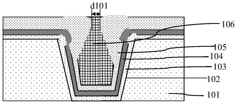
[0056] Such as image 3 As shown, it is a schematic structural view of the copper-filled groove structure of the embodiment of the present invention; the copper-filled groove structure of the embodiment of the present invention includes:

[0057] The groove 2 is formed in the first dielectric layer 1 .

[0058] A barrier layer 3 is formed on the bottom surface and side surfaces of the groove 2 .

[0059] In the embodiment of the present invention, the barrier layer 3 is a TaN layer, and in other embodiments, the barrier layer 3 can also be a TiN layer.

[0060] A cobalt layer 4 is formed on the surface of the barrier layer 3 , and a ruthenium layer 5 is formed on the surface of the cobalt layer 4 .

[0061] The copper layer 6 completely fills the groove 2 formed with the barrier layer 3 , the cobalt layer 4 and the ruthenium layer 5 and forms a copper-filled groove structure.

[0062] The copper layer 6 is entirely composed of copper electroplated film.

[0063] The cobalt...


PUM


Abstract

The invention discloses a copper-filled groove structure, and the structure comprises a groove which is formed in a first dielectric layer; barrier layers are formed on the bottom surface and the side surface of the groove; forming a cobalt layer and a ruthenium layer on the surface of the barrier layer; the copper layer completely fills the groove in which the barrier layer, the cobalt layer and the ruthenium layer are formed and forms a copper filling groove structure; the copper layer is completely composed of a copper electroplating film; a cobalt layer and a ruthenium layer are overlapped to form an auxiliary nucleation film layer of the copper layer. The invention further discloses a manufacturing method of the copper filling groove structure. The copper layer does not contain a copper seed crystal layer and is completely composed of the copper electroplating film, so that the capacity of filling copper in the groove can be improved, the structure of the groove filled with the copper can be reduced, and the copper electroplating film is particularly suitable for being used as a copper connecting wire and a through hole below 14 nm process nodes.

Description

technical field [0001] The invention relates to the manufacturing field of semiconductor integrated circuits, in particular to a copper-filled groove structure. The invention also relates to a method of manufacturing a copper-filled groove structure. Background technique [0002] As the critical dimension (CD) of the back-end (BEOL) copper interconnection becomes smaller and smaller, it becomes more and more difficult to fill the trench (Trench) and via (via) openings, which are explained as follows: [0003] Such as figure 1 As shown, it is a structural schematic diagram of the copper-filled groove structure formed by the first existing copper-filled groove structure manufacturing method; the existing first copper-filled groove structure manufacturing method adopts physical vapor deposition (PVD) TaN +Ta+ copper seed layer (Cu Seed) process, including the following steps: [0004] A groove 102 is formed on a dielectric layer such as an interlayer film 101 , and the groov...

Claims


Application Information

Patent Timeline
Patent Type & Authority Applications(China)
IPC IPC(8): H01L23/528H01L23/532H01L21/768
CPCH01L23/528H01L23/53209H01L21/76843H01L21/76871H01L21/76877H01L2221/1068H01L2221/1084H01L21/76873H01L23/53238H01L21/76846H01L2221/1089H01L23/5226H01L21/02458
Inventor 曾招钦鲍宇
Owner SHANGHAI HUALI INTEGRATED CIRCUTE MFG CO LTD
Why Eureka
Try Eureka