ESD protection structure and preparation method thereof

A technology of ESD protection and control gate, applied in semiconductor/solid-state device manufacturing, semiconductor devices, electrical components, etc., can solve the problem of high static leakage and achieve the effect of ultra-low leakage

Active Publication Date: 2022-05-31
MICROTERA SEMICON (GUANGZHOU) CO LTD
View PDF5 Cites 0 Cited by
  • Summary
  • Abstract
  • Description
  • Claims
  • Application Information

AI Technical Summary

Problems solved by technology

[0004] In view of the above-mentioned shortcoming of the prior art, the object of the present invention is to provide a kind of ESD protection structure and preparation method thereof, be used to solve the problem that the static electric leakage of existing ESD protection structure is higher

Method used


Image

  • ESD protection structure and preparation method thereof
  • ESD protection structure and preparation method thereof
  • ESD protection structure and preparation method thereof

Examples


Embodiment 1

[0044] As shown in FIG. 4, this embodiment provides an N-type ESD protection structure, the N-type ESD protection structure includes: full consumption

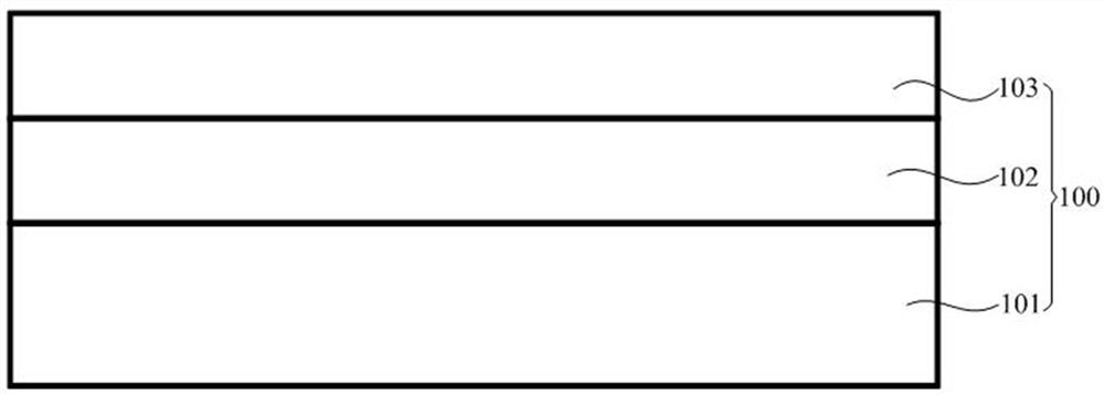
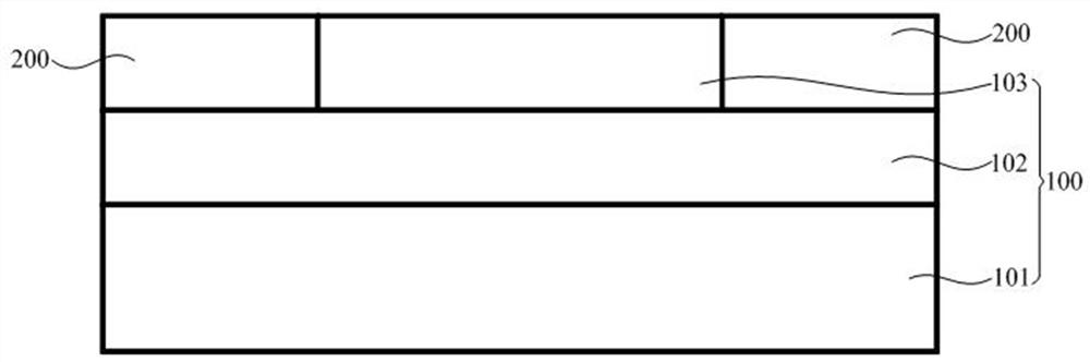
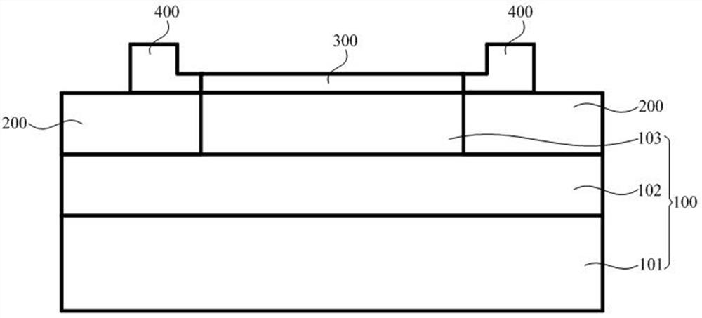
[0045] The fully depleted silicon-on-insulator 100 sequentially includes a silicon substrate 101, a buried oxide layer 102 and a top layer of silicon from bottom to top

[0046] The silicide layer 200 is formed on the upper surface of the buried oxide layer 102, and is formed on both sides of the top layer silicon 103

[0047] Specifically, the silicide layer 200 sequentially includes silicide and metal silicide (not shown in the figure) from bottom to top,

[0048] The gate oxide layer 300 is formed on the upper surface of the top layer silicon 103.

[0049] Specifically, the gate oxide layer 300 is a silicon oxide layer or a hafnium oxide layer. In this embodiment, the gate oxide layer 300 is made of oxygen

[0050] The isolation layer 400 is formed on a part of the upper surface of the silicide layer 200, and is formed on the ga...

Embodiment 2

[0074] This embodiment provides a P-type ESD protection structure, the difference between the structure and the first embodiment is that the top layer silicon

[0075] In the P-type ESD protection structure of this embodiment, when performing ESD protection, the drain 800 is connected to the negative electrode as a cathode


PUM

PropertyMeasurementUnit
thicknessaaaaaaaaaa
thicknessaaaaaaaaaa
thicknessaaaaaaaaaa

Abstract

The invention provides an ESD protection structure, comprising: fully depleted silicon-on-insulator, including a silicon substrate, a buried oxide layer and a top layer of silicon from bottom to top; a silicide layer, formed on the upper surface of the buried oxide layer, and formed on the top layer Both sides of silicon; gate oxide layer, formed on the upper surface of the top layer of silicon; isolation layer, formed on the upper surface of part of the silicide layer, and formed on both sides of the gate oxide layer; control gate, formed on part of the gate oxide layer The upper surface; the programmable gate is formed on the upper surface of part of the gate oxide layer and part of the isolation layer adjacent to it, and is formed on both sides of the control gate, wherein there is a distance between the programmable gate and the control gate; the source is formed on The upper surface of the silicide layer on the top silicon side is formed on the side of the isolation layer away from the programmable gate; the drain is formed on the upper surface of the silicide layer on the other side of the top silicon and is formed on the isolation layer away from the programmable gate. side of the programming gate. Through the ESD protection structure provided by the invention, the problem of high static leakage in the existing structure is solved.

Description

ESD protection structure and preparation method thereof technical field [0001] The present invention relates to the field of semiconductors, in particular to a ESD protection structure and a preparation method thereof. Background technique [0002] The electrostatic protection (Electrostatic discharge, ESD) of the chip has always been a very important link. Structures such as thyristor protection can make the chip resistant to ESD, but these devices have high static leakage (when the chip is working normally static leakage of ESD devices), it is difficult to meet the needs of ultra-low leakage, such as ultra-low bias current amplifiers and other high-precision instrumentation amplifiers leakage requirements of the amplifier. Therefore, designing a kind of ultra-low leakage ESD protection structure has become an urgent need for those skilled in the art to solve one of the technical problems. SUMMARY OF THE INVENTION In view of the shortcoming of the above-mentione...

Claims


Application Information

Patent Timeline
Patent Type & Authority Patents(China)
IPC IPC(8): H01L27/02H01L27/12H01L21/84
CPCH01L27/0266H01L27/1203H01L21/84
Inventor 刘尧李建平刘筱伟班桂春刘海彬刘森
Owner MICROTERA SEMICON (GUANGZHOU) CO LTD
Why Eureka
Try Eureka