Semiconductor structure and chip packaging method

A chip packaging and semiconductor technology, applied in the direction of semiconductor devices, semiconductor/solid-state device manufacturing, semiconductor/solid-state device components, etc., can solve the problems of increasing system complexity and cost, insufficient improvement, and inability to meet the needs of use, and achieve occupation Small space, short traces, and low cost

Pending Publication Date: 2022-05-06
杭州云合智网技术有限公司
View PDF0 Cites 0 Cited by
  • Summary
  • Abstract
  • Description
  • Claims
  • Application Information

AI Technical Summary

Problems solved by technology

There are also some methods that mix the above methods, but in general, either the improvement is not enough, or the complexity and cost of the system are greatly increased, so it cannot meet the use requirements

Method used


Image

  • Semiconductor structure and chip packaging method
  • Semiconductor structure and chip packaging method
  • Semiconductor structure and chip packaging method

Examples


Embodiment Construction

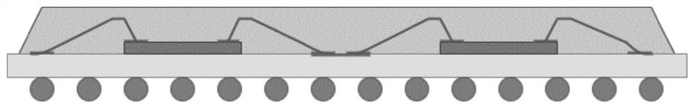
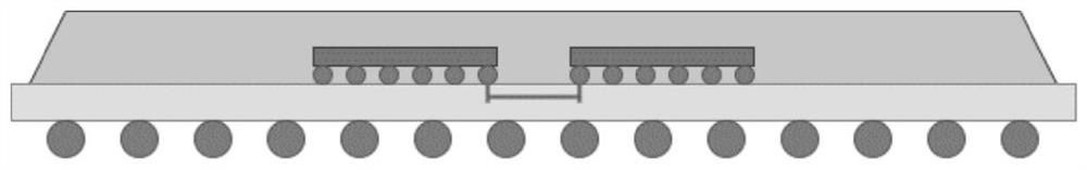
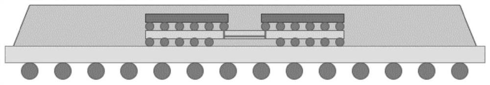
[0044] The following will clearly and completely describe the technical solutions in the embodiments of the present invention with reference to the accompanying drawings in the embodiments of the present invention. Obviously, the described embodiments are only some, not all, embodiments of the present invention. Based on the embodiments of the present invention, all other embodiments obtained by persons of ordinary skill in the art without making creative efforts belong to the protection scope of the present invention.

[0045] In order to better understand the technical solutions of the present invention, the embodiments of the present invention will be described in detail below in conjunction with the accompanying drawings.

[0046] It should be clear that the described embodiments are only some of the embodiments of the present invention, not all of them. Based on the embodiments of the present invention, all other embodiments obtained by persons of ordinary skill in the ar...


PUM


Abstract

The invention provides a semiconductor structure and a chip packaging method. The semiconductor structure comprises a substrate, a first chip and a second chip, wherein the first chip and the second chip are arranged on the substrate in parallel; wherein the first chip and the second chip are interconnected directly through a lead bonding process; moreover, for the pins, where high-speed signals need to pass, between the first chip and the second chip, the pins are configured to be oppositely arranged and are connected through parallel routing. According to the embodiment of the invention, through a lead bonding technology between chips, the circuit is shorter in routing, small in occupied space, better in performance of high-speed signals, free of too much change in cost, and even lower in cost. Compared with 2.5 D and 3D packaging, the cost of the embodiment is much lower, the requirement for manufacturing equipment is not high, and the method is very suitable for large-scale production.

Description

technical field [0001] The invention relates to the field of semiconductor packaging, in particular to a semiconductor structure and a chip packaging method. Background technique [0002] With the development of semiconductor technology, the scale of the chip is getting larger and larger, and the chip integrated on the package is also becoming more and more complex. When packaging, it is often necessary to integrate a variety of different chips, such as memory + logic chips, optoelectronics + electronic components, etc., through packaging, 3D stacking and other technologies to achieve smaller volume and power consumption. [0003] In some applications, for chips with fewer input and output pins, if two chips need to be interconnected, the general methods are: [0004] 1. Use wire bonding, and then connect through the package substrate (Substrate). [0005] Wire bonding technology is the main technology of traditional packaging, which has the advantages of low cost, high re...

Claims


Application Information

Patent Timeline
Patent Type & Authority Applications(China)
IPC IPC(8): H01L23/498H01L23/49H01L21/50H01L21/60
CPCH01L23/49811H01L24/48H01L24/49H01L21/50H01L24/85H01L2224/48091H01L2224/48135H01L2224/48137H01L2224/4912H01L2224/49175H01L2224/85H01L2224/16145H01L2924/181H01L2224/48227H01L2224/49171H01L2924/15311H01L2224/73257H01L2224/16225H01L2924/00012
Inventor 舒伟峰陈清华
Owner 杭州云合智网技术有限公司
Why Eureka
Try Eureka