Check patentability & draft patents in minutes with Patsnap Eureka AI!

Layout processing method, layout processing system and electronic equipment

A processing method and layout technology, applied in the direction of electrical digital data processing, special data processing applications, computer-aided design, etc., can solve problems such as difficult automatic design, difficult parameter adjustment, and weak scalability, so as to improve scalability, The effect of improving flexibility

Pending Publication Date: 2022-05-10
CHANGXIN MEMORY TECH INC
View PDF0 Cites 0 Cited by
  • Summary
  • Abstract
  • Description
  • Claims
  • Application Information

AI Technical Summary

Problems solved by technology

Full custom design can better improve device performance, but it is time-consuming, and it is difficult to fully realize automatic design. The layout is usually of fixed size, its parameters are difficult to adjust, and the scalability is weak

Method used


Image

  • Layout processing method, layout processing system and electronic equipment
  • Layout processing method, layout processing system and electronic equipment
  • Layout processing method, layout processing system and electronic equipment

Examples


Embodiment Construction

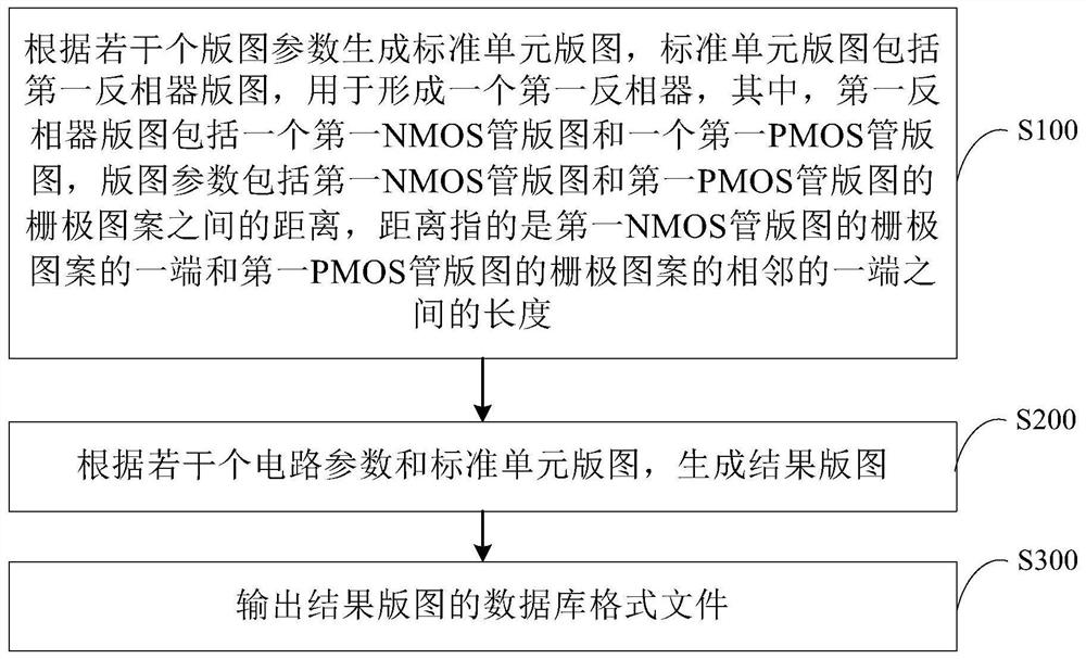
[0046] An embodiment of the present disclosure provides a layout processing method, which generates a standard cell layout according to several layout parameters, and generates a resulting layout according to several circuit parameters and the standard cell layout. By adjusting the layout parameters, the length between the gate pattern of the first NMOS transistor layout and the gate pattern of the first PMOS transistor layout in the standard cell layout can be adjusted. The formed circuit structure can obtain different result layouts, improve the scalability of the layout, and realize automatic design.

[0047] In order to make the above objects, features and advantages of the embodiments of the present disclosure more obvious and understandable, the technical solutions in the embodiments of the present disclosure will be clearly and completely described below in conjunction with the accompanying drawings in the embodiments of the present disclosure. Apparently, the described...


PUM


Abstract

The invention provides a layout processing method, a layout processing system and electronic equipment, relates to the technical field of semiconductors, and is used for solving the technical problem that layout expandability is weak. The layout processing method comprises the steps that a standard unit layout is generated according to a plurality of layout parameters, and the standard unit layout comprises a first phase inverter layout and a second phase inverter layout; the first phase inverter layout is used for forming a first phase inverter, the first phase inverter layout comprises a first NMOS (N-channel Metal Oxide Semiconductor) tube layout and a first PMOS (P-channel Metal Oxide Semiconductor) tube layout, and layout parameters comprise the distance between gate patterns of the first NMOS tube layout and the first PMOS tube layout; generating a result layout according to the plurality of circuit parameters and the standard unit layout; and outputting a database format file of the result layout. The layout parameters are adjusted to adjust the lengths of the ends, close to each other, of the gate patterns of the first NMOS transistor layout and the first PMOS transistor layout, the circuit parameters are adjusted to adjust the circuit structure formed by the standard unit layout, and the expandability of the layout is improved.

Description

technical field [0001] The present disclosure relates to the technical field of semiconductors, and in particular to a layout processing method, a layout processing system and electronic equipment. Background technique [0002] CMOS (Complementary Metal Oxide Semiconductor, Chinese: Complementary Metal Oxide Semiconductor) digital IC (Integrated Circuit, Chinese: Integrated Circuit) design can usually be divided into full-custom (Full-custom) design and semi-custom (Semi-custom) design. Full-custom design is a transistor-level based design methodology where all components, interconnects, and layout of a circuit are designed directly. Full-custom design can better improve device performance, but it is time-consuming, and it is difficult to fully realize automatic design. The layout is usually of fixed size, its parameters are difficult to adjust, and the scalability is weak. Contents of the invention [0003] Embodiments of the present disclosure provide a layout processin...

Claims


Application Information

Patent Timeline
IPC IPC(8): G06F30/392
CPCG06F30/392
Inventor 徐帆
Owner CHANGXIN MEMORY TECH INC
Features
  • R&D
  • Intellectual Property
  • Life Sciences
  • Materials
  • Tech Scout
  • Unparalleled Data Quality
  • Higher Quality Content
  • 60% Fewer Hallucinations
Learn More