MEMS (Micro Electro Mechanical System) capacitor-embedded resistor-embedded package loading plate and manufacturing process thereof

A technology of encapsulating carrier boards and manufacturing processes, which is applied in the directions of multilayer circuit manufacturing, printed circuit manufacturing, and printed circuits connected with non-printed electrical components. Poor effect and other problems, to achieve the effect of increasing volume, improving sensitivity and signal-to-noise ratio, and improving alignment

Pending Publication Date: 2022-05-10
JIANGSU PROVISION ELECTRONICS CO LTD
View PDF0 Cites 0 Cited by
  • Summary
  • Abstract
  • Description
  • Claims
  • Application Information

AI Technical Summary

Problems solved by technology

At present, some MEMS carrier boards are made by overlapping three-layer PCB boards. The three-layer PCB boards are laminated to form a cavity, and the metal surface is plated on the second layer PCB board to form a shielding cavity. This package has poor shielding effect. And the volume of the back cavity is small, and the signal-to-noise ratio of the product is low

Method used


Image

  • MEMS (Micro Electro Mechanical System) capacitor-embedded resistor-embedded package loading plate and manufacturing process thereof
  • MEMS (Micro Electro Mechanical System) capacitor-embedded resistor-embedded package loading plate and manufacturing process thereof
  • MEMS (Micro Electro Mechanical System) capacitor-embedded resistor-embedded package loading plate and manufacturing process thereof

Examples


Embodiment

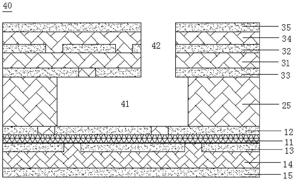
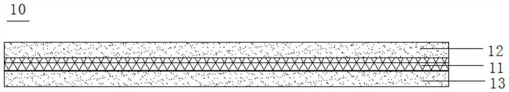
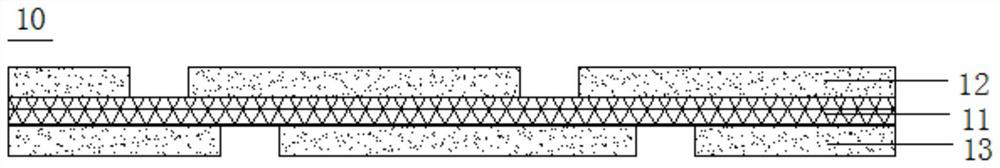
[0057] Example: as Figure 1-11 As shown, a manufacturing process of a MEMS buried capacitance and buried resistance package carrier board includes the following steps:

[0058] Step 1: Prepare three core boards, namely the first core board 10 , the second core board 20 and the third core board 30 , wherein, such as figure 2 As shown, the first core board 10 includes a capacitor layer 11 and a first copper foil layer 12 and a second copper foil layer 13 respectively disposed on the front and back sides of the capacitor layer, such as Figure 5 As shown, the second core board 20 includes a second insulating layer 21 and a fourth copper foil layer 22 and a fifth copper foil layer 23 respectively disposed on the front and back sides of the second insulating layer, such as Figure 8 As shown, the third core board 30 includes a third insulating layer 31 and a sixth copper foil layer 32 and a seventh copper foil layer 33 respectively disposed on the front and back sides of the thi...


PUM


Abstract

The invention relates to an MEMS (Micro Electro Mechanical System) capacitor-embedded resistor-embedded packaging carrier plate and a manufacturing process thereof, and the process comprises the following steps: preparing three core plates, namely a first core plate, a second core plate and a third core plate; an inner layer circuit of the first core board; pressing the first core plate; etching a second core plate and pressing a film; grooving the film plate; an inner layer circuit of the third core board; pressing a third core plate; laminating a plurality of layers of boards; and uncovering: after drilling and copper plating, outer layer circuit, solder mask and surface treatment are carried out on the semi-finished product board, laser uncovering treatment is carried out on the third core board to form a sound hole, and a finished product packaging carrier board is obtained. The packaging substrate obtained by the invention not only realizes the function of burying the capacitor and the resistor, but also increases the volume of the back cavity under the condition of not increasing the volume of the device, improves the sensitivity and the signal-to-noise ratio of the product, and accords with the development trend of device miniaturization.

Description

technical field [0001] The invention relates to a MEMS package carrier, in particular to a MEMS buried capacitance and buried resistance package carrier and a manufacturing process thereof. Background technique [0002] The development of MEMS (Microelectromechanical Systems) technology and process in the past three decades, especially the development of MEMS technology based on silicon chips, has realized the miniaturization and low cost of many sensors (such as pressure sensors, accelerometers, gyroscopes, etc.). At present, some MEMS carrier boards are made by overlapping three-layer PCB boards. The three-layer PCB board is laminated to form a cavity, and the metal surface is plated on the second-layer PCB board to form a shielding cavity. This packaging has poor shielding effect. And the volume of the back cavity is small, and the signal-to-noise ratio of the product is low. SUMMARY OF THE INVENTION [0003] In order to overcome the above-mentioned defects, the presen...

Claims


Application Information

Patent Timeline
IPC IPC(8): H05K1/14H05K1/18H05K3/46
CPCH05K1/183H05K3/4611H05K1/14
Inventor 马洪伟张志礼
Owner JIANGSU PROVISION ELECTRONICS CO LTD
Why Eureka
Try Eureka