Wafer thinning and polishing device

A technology for thinning polishing and wafers, which is applied to grinding drive devices, grinding/polishing equipment, and surface polishing machine tools, etc. It can solve problems such as affecting the polishing effect, slow conversion speed, and uneven liquid, so as to improve polishing effect, fast switching speed, and the effect of improving spray uniformity

Active Publication Date: 2022-05-13
四川明泰微电子科技股份有限公司
View PDF12 Cites 2 Cited by
  • Summary
  • Abstract
  • Description
  • Claims
  • Application Information

AI Technical Summary

Problems solved by technology

[0003] There are many problems in the existing technology: the method of manual glue application is low in efficiency; several sets of complex modules are used for rough grinding, fine grinding and polishing, the equipment cost is high, and the switching speed between steps is slow; when polishing, only Spray the polishing liquid on one position of the circle, the liquid is not uniform, which will affect the polishing effect

Method used


Image

  • Wafer thinning and polishing device
  • Wafer thinning and polishing device
  • Wafer thinning and polishing device

Examples


Embodiment Construction

[0034] The present application will be described in detail below with reference to the accompanying drawings and embodiments. It should be noted that, in the case of no conflict, the embodiments in the present application and the features in the embodiments can be combined with each other.

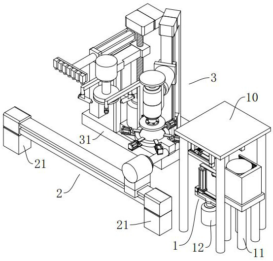
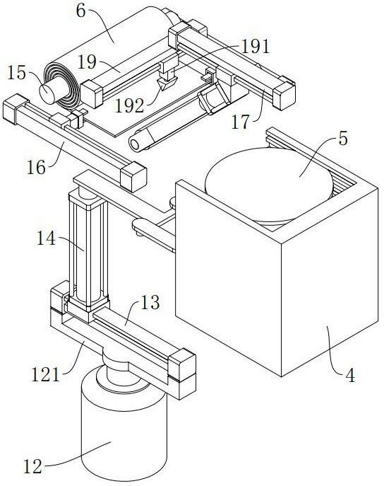
[0035] Such as Figure 1~Figure 9 A wafer thinning and polishing device shown includes a glue application unit 1 , a transport unit 2 , and a thinning and polishing unit 3 .

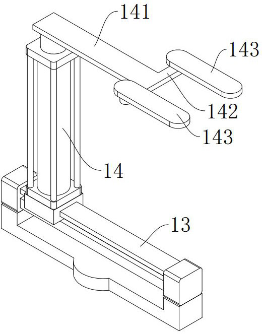
[0036] The gluing unit 1 comprises a top frame 10 and a bottom frame 11 located at the lower end, the bottom frame 11 is provided with a wafer frame 4 for placing a plurality of wafers 5, and one side of the bottom frame 11 is provided with a vertically arranged first rotating Motor 12, one end of its output shaft is provided with a bracket 121, the upper end of the bracket 121 is provided with a first rodless linear cylinder 13, and the upper end of its sliding end is provided with a vertically arranged first uniax...


PUM


Abstract

A wafer thinning and polishing device comprises a rubberizing unit, a conveying unit and a thinning and polishing unit. The rubberizing unit is used for rubberizing the front surface of the wafer. The conveying unit is arranged on one side of the rubberizing unit and used for overturning and conveying the rubberized wafers. The thinning and polishing unit is arranged on one side of the conveying unit and comprises a sixth rodless linear air cylinder, a third rotating motor is arranged on one side of the sliding end of the sixth rodless linear air cylinder, a combined frame is arranged at one end of an output shaft of the third rotating motor, a pair of fourth rotating motors is arranged on the combined frame, grinding discs are arranged on output shafts of the third rotating motor, one grinding disc is a coarse grinding disc, and the other grinding disc is a fine grinding disc. A fifth rotating motor is arranged on one side face of a sliding block of the lead screw lifting assembly, a polishing wheel is arranged at one end of an output shaft of the fifth rotating motor, two sets of liquid spraying pipes are arranged on the two sides of the lead screw lifting assembly, and a plurality of laser distance measuring sensors are further arranged on one side of the lead screw lifting assembly. The wafer thinning and polishing device provided by the invention can be used for automatically gluing and transporting, and is simple in structure, low in equipment cost, high in thinning and polishing precision and relatively good in thickness uniformity of polished wafers.

Description

technical field [0001] The invention relates to the technical field of semiconductor product manufacturing, in particular to a wafer thinning and polishing device. Background technique [0002] In the manufacture of semiconductor products, wafers need to be used. In order to ensure that the wafers maintain sufficient strength during testing and transportation, the wafers shipped from the wafer factory are relatively thick. Before the wafer is used, it needs to be thinned and polished to meet the requirements of improving its heat dissipation efficiency, reducing the chip packaging volume, and improving electrical performance. The thinning and polishing process includes four steps: (1) Paste glue on the front of the wafer to protect the circuit when the back of the wafer is being ground; (3) Fine grinding: Grinding with a grinding disc with a smaller particle size, the efficiency is reduced, the precision is improved, and the damage of coarse grinding can be reduced; (4) Pol...

Claims


Application Information

Patent Timeline
Patent Type & Authority Applications(China)
IPC IPC(8): B24B29/02B24B41/00B24B57/02B24B27/00B24B49/12B24B47/12B24B7/22B24B41/02B24B41/06
CPCB24B29/02B24B41/005B24B57/02B24B27/0076B24B49/12B24B47/12B24B7/228B24B41/02B24B41/068Y02P70/50
Inventor 李蛇宏杨益东
Owner 四川明泰微电子科技股份有限公司
Why Eureka
Try Eureka