CMOS (complementary metal oxide semiconductor) inverter mold for teaching

A technology of inverters and molds, applied in the field of CMOS inverter molds for teaching, can solve the problems of being unable to intuitively understand and view the structure and manufacturing process of CMOS inverters, so as to improve learning interest and learning efficiency, and improve production efficiency , The effect of saving printing costs

Pending Publication Date: 2022-05-13
CHONGQING COLLEGE OF ELECTRONICS ENG
View PDF4 Cites 0 Cited by
  • Summary
  • Abstract
  • Description
  • Claims
  • Application Information

AI Technical Summary

Problems solved by technology

The manufacturing process of CMOS inverters is a skill point that students majoring in integrated circuits need to master. In the existing integrated circuit teaching process, teaching explanations are usually given through PPT, and students cannot intuitively understand and view the structure and manufacturing process of CMOS inverters.

Method used


Image

  • CMOS (complementary metal oxide semiconductor) inverter mold for teaching
  • CMOS (complementary metal oxide semiconductor) inverter mold for teaching
  • CMOS (complementary metal oxide semiconductor) inverter mold for teaching

Examples


Embodiment 1

[0037] Embodiment 1 is basically as attached figure 1 Shown:

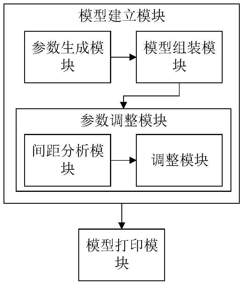
[0038] A CMOS inverter mold for teaching, such as figure 1 As shown, it includes model building module and model printing module. The model building module includes a parameter generation module, a model assembly module and a parameter adjustment module.

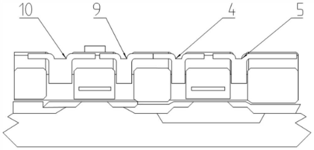
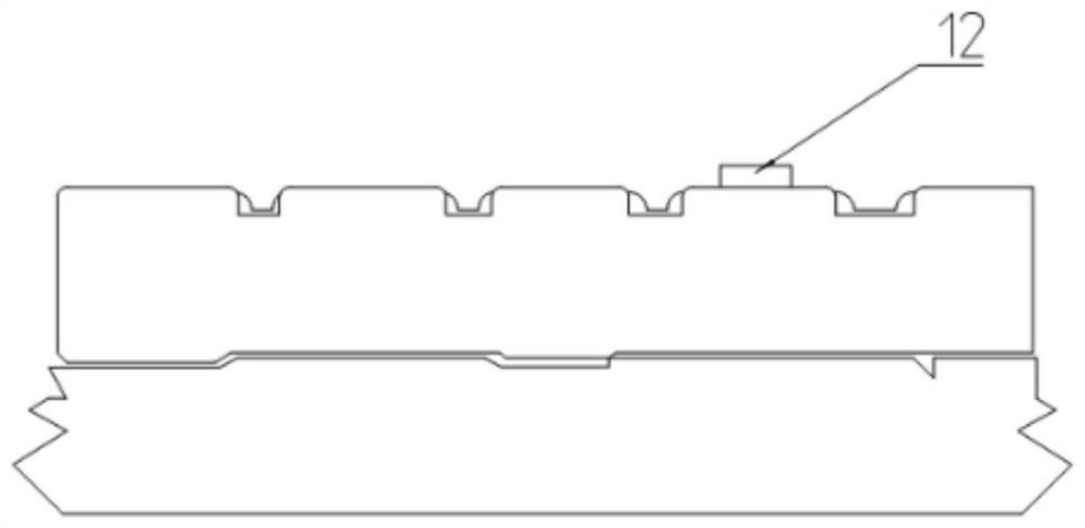
[0039] The parameter generation module is used to generate mold parameters of several mold parts. In this embodiment, the mold part includes a P-type substrate 1, an N-type hydrazine structure 2, an N+ injection region 3, an N-type drain electrode 4, an N-type source electrode 5, an N-type gate region 6, a P-type Hydrazine structure 7 , P+ injection region 8 , P-type drain electrode 9 , P-type source electrode 10 , P-type gate region 11 and gate electrode 12 . The mold parameters include the shape, size and color of each mold part. In this embodiment, the colors of each mold part are different, so as to distinguish each mold part. Wherein, the N-type drain e...


PUM


Abstract

The invention relates to the technical field of teaching aid preparation, in particular to a CMOS (complementary metal oxide semiconductor) inverter mold for teaching, which comprises a model building module and a model printing module, the model establishing module comprises a parameter generating module, a model assembling module and a parameter adjusting module; the parameter generation module is used for generating mold parameters of a plurality of mold parts; the model assembly module is used for assembling mold parts according to the mold parameters generated by the parameter generation module and generating an assembly effect schematic diagram; the parameter adjustment module is used for adjusting the mold parameters generated by the parameter generation module according to the assembly effect schematic diagram and generating the adjusted mold parameters; and the model printing module is used for printing mold parts according to the adjusted mold parameters. By adopting the scheme, the structure of the CMOS inverter can be clearly presented, the structure of the CMOS inverter is convenient to master, and the learning interest and learning efficiency are improved.

Description

technical field [0001] The invention relates to the technical field of teaching aid preparation, in particular to a CMOS inverter mold for teaching. Background technique [0002] The inverter can invert the phase of the input signal by 180 degrees. This circuit is used in analog circuits, such as audio amplifiers, clock oscillators, etc. In the design of integrated circuits, inverters are often used. The CMOS inverter is the core device of all digital integrated circuit designs. It has the advantages of large noise margin, extremely high input resistance, extremely low static power consumption, and insensitivity to noise and interference, so it is widely used in digital in integrated circuits. The manufacturing process of CMOS inverters is a skill point that students majoring in integrated circuits need to master. In the existing integrated circuit teaching process, teaching explanations are usually given through PPT, and students cannot intuitively understand and view the...

Claims


Application Information

Patent Timeline
Patent Type & Authority Applications(China)
IPC IPC(8): G09B25/00
CPCG09B25/00
Inventor 卢静刘睿强陈方毅冯筱佳瞿豪余志林马心沂
Owner CHONGQING COLLEGE OF ELECTRONICS ENG
Why Eureka
Try Eureka