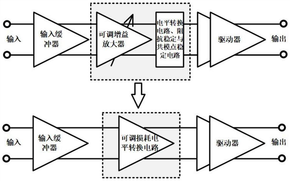
Level converter with adjustable loss
A level shifter and current technology, applied to amplifiers with semiconductor devices/discharge tubes, amplifiers, electrical components, etc., can solve problems such as high common-mode points and complex circuit structures, and achieve the goal of reducing common-mode levels Effect
- Summary
- Abstract
- Description
- Claims
- Application Information
AI Technical Summary
Problems solved by technology
Method used
Image

Examples
Embodiment 1
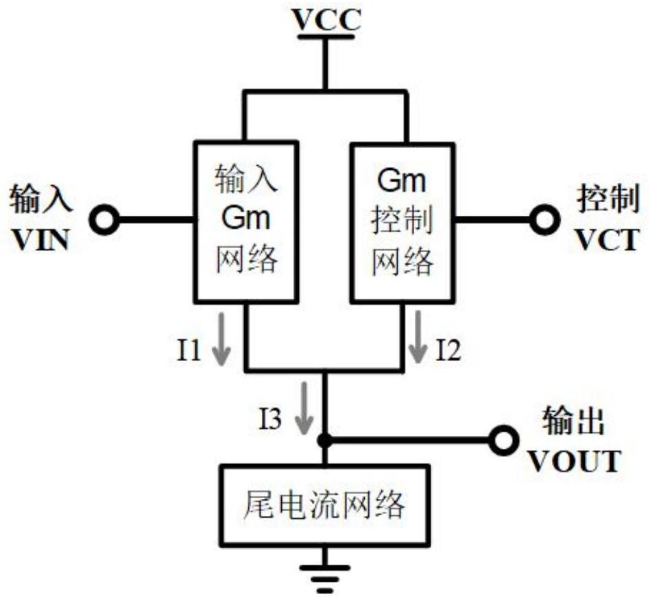
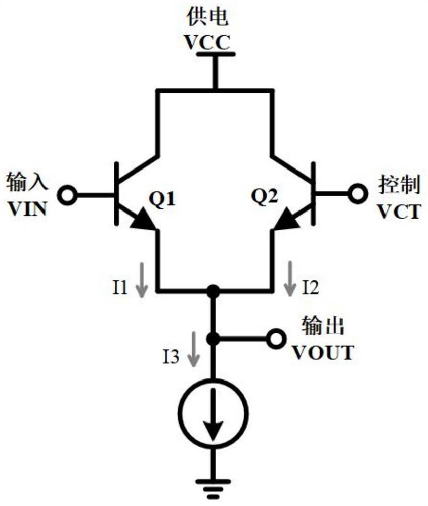
[0044] image 3 is the adjustable loss level shifter provided in this embodiment, including a first transistor Q1, a second transistor Q2 and a tail current source;
[0045] The base of the first transistor Q1 is connected to the input signal VIN, and the emitter is connected to the output voltage VOUT; the base of the second transistor Q2 is connected to the control voltage VCT, and the emitter is connected to the output voltage VOUT; the collectors of the first transistor Q1 and the second transistor Q2 are connected to the power supply Voltage VCC; the tail current source provides the total operating current I3 for the first transistor Q1 and the second transistor Q2;
[0046] Further preferably, the sum of the current I1 flowing through the first transistor Q1 and the current I2 of the second transistor Q2 is the tail current source current I3, and I3 remains unchanged during the circuit control process;
[0047] Further preferably, when the input signal reaches VOUT thro...
Embodiment 2
[0052] like Figure 7 As shown, the adjustable loss level shifter provided in this embodiment includes a first transistor Q1, a second transistor Q2, a third transistor Q3, a fourth transistor Q4 and a tail current source; the first transistor Q1 is directly connected to the input VIN node , the third transistor Q3 is connected to the input node through the capacitor C1, the function of the capacitor C1 is to isolate the DC signal from VIN, and prevent the breakdown of the base voltage of the third transistor Q3 from being too high; the second transistor Q2 adopts a diode connection in the circuit, The purpose is to reduce the voltage drop across the fourth transistor Q4 and prevent breakdown caused by the collector voltage of the fourth transistor Q4 being too high;
[0053] Compared with embodiment 1, at first, the input Gm network part of embodiment 2 has increased the 3rd transistor Q3, has improved the transconductance value of whole network, has reduced circuit absolute ...
PUM
 Abstract
Description
Claims
Application Information
 - Generate Ideas
- Intellectual Property
- Life Sciences
- Materials
- Tech Scout
- Unparalleled Data Quality
- Higher Quality Content
- 60% Fewer Hallucinations
Browse by: Latest US Patents, China's latest patents, Technical Efficacy Thesaurus, Application Domain, Technology Topic, Popular Technical Reports.
© 2025 PatSnap. All rights reserved.Legal|Privacy policy|Modern Slavery Act Transparency Statement|Sitemap|About US| Contact US: help@patsnap.com