Epitaxial structure of red and yellow GaAs diode and preparation method thereof

An epitaxial structure and diode technology, applied in the direction of final product manufacturing, sustainable manufacturing/processing, climate sustainability, etc., can solve the problems of insufficient simplification of epitaxial structure and epitaxial processing technology, affecting LED luminous brightness, affecting light reflection, etc. , to achieve the effects of low production cost, simplified epitaxial structure and epitaxial processing technology, and increased spontaneous emission

Pending Publication Date: 2022-05-24
JIANGXI ZHAO CHI SEMICON CO LTD
View PDF0 Cites 1 Cited by
  • Summary
  • Abstract
  • Description
  • Claims
  • Application Information

AI Technical Summary

Problems solved by technology

[0003] The epitaxy of the LED chip requires multi-layer growth. The epitaxial structure of the current red and yellow GaAs LED front-mounted positive polarity chip contains an N-type claddin

Method used


Image

  • Epitaxial structure of red and yellow GaAs diode and preparation method thereof
  • Epitaxial structure of red and yellow GaAs diode and preparation method thereof
  • Epitaxial structure of red and yellow GaAs diode and preparation method thereof

Examples


Embodiment 1

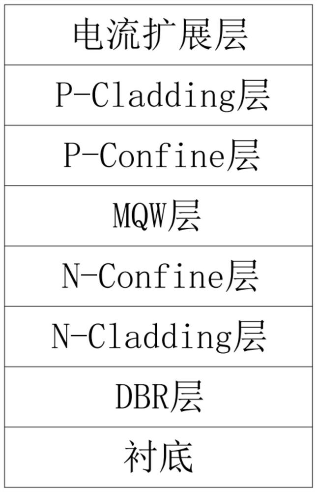
[0035] like figure 1 shown, figure 1 It is the epitaxial structure of the traditional red-yellow GaAs diode. Multiple quantum well layer (Multiple Quantum Well, MQW layer for short), P-type confinement layer (P-Confine layer), P-type cladding layer (P-Cladding layer) and current spreading layer, the existence of N-type cladding layer not only makes the epitaxial structure And the epitaxial processing technology is not simple enough, and because the travel of photons to the Bragg reflector is increased, the reflection of light by the Bragg reflector is affected, and then the luminous brightness of the LED is affected.

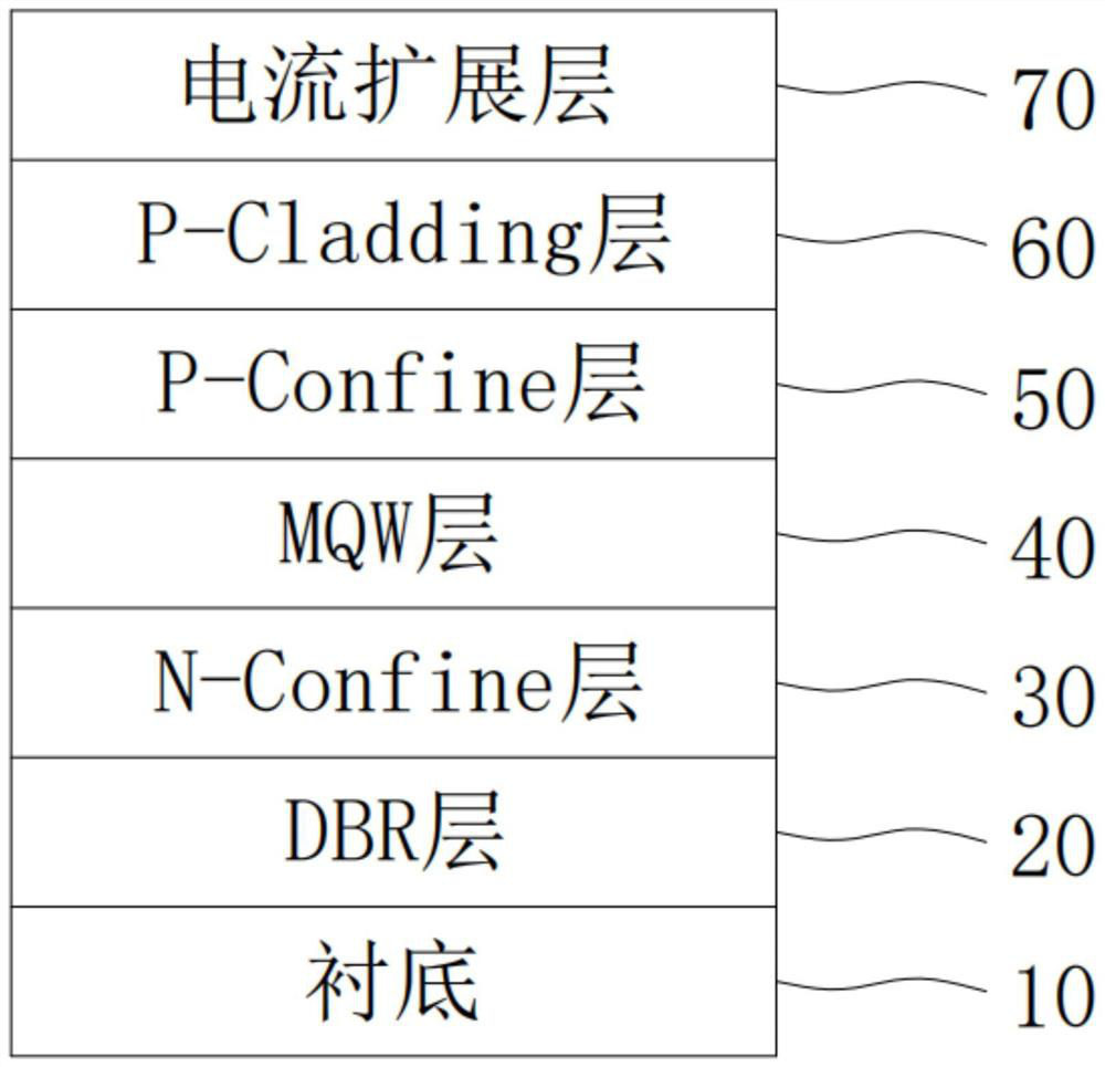
[0036] like figure 2 As shown, an embodiment of the present invention provides an epitaxial structure of a red-yellow GaAs diode. The epitaxial structure includes: a substrate 10, a Bragg mirror 20 and an N-type confinement layer 30 that are sequentially grown upward on the substrate 10. , the multiple quantum well layer 40, the P-type confinement layer 50, ...

Embodiment 2

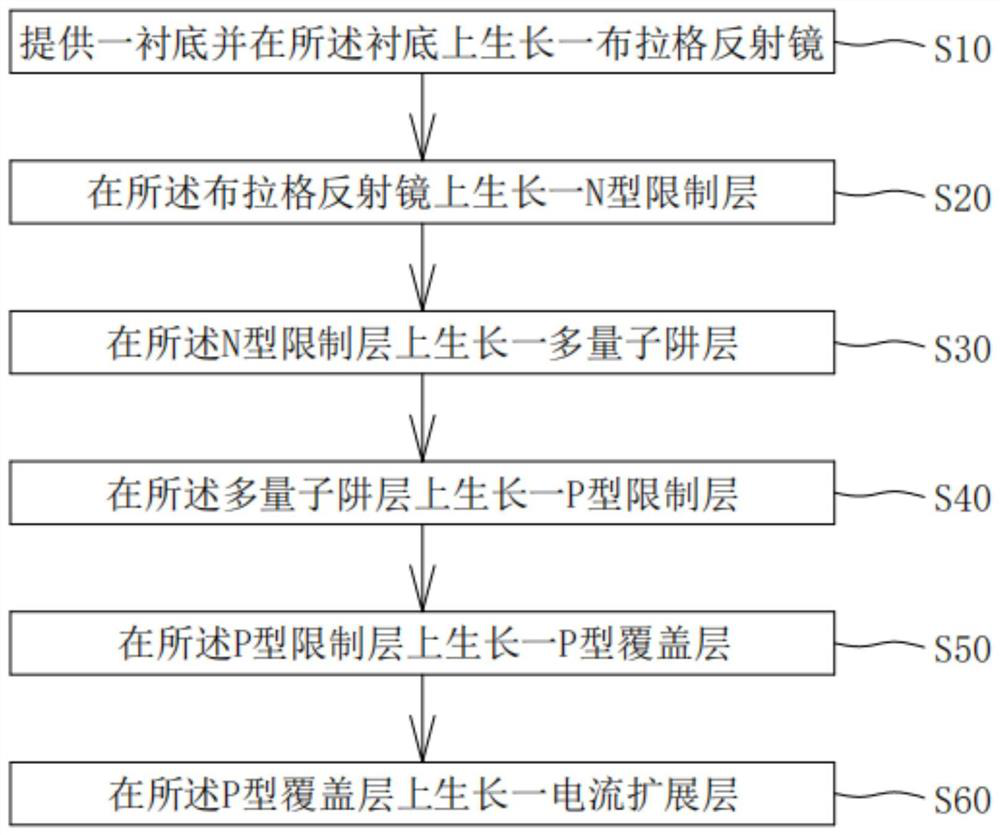
[0044] Please refer to image 3 , the second embodiment of the present invention provides a method for preparing an epitaxial structure of a red-yellow GaAs diode, which is used for preparing the epitaxial structure of the red-yellow GaAs diode in the above-mentioned first embodiment, and the preparation method includes steps S10-S60 :

[0045] S10, providing a substrate and growing a Bragg mirror on the substrate;

[0046] S20, growing an N-type confinement layer on the Bragg mirror;

[0047] S30, growing a multiple quantum well layer on the N-type confinement layer;

[0048] S40, growing a P-type confinement layer on the multiple quantum well layer;

[0049] S50, growing a P-type capping layer on the P-type confinement layer;

[0050] S60, growing a current spreading layer on the P-type cladding layer;

[0051] In the embodiment of the present invention, the N-type confinement layer is an AlGaInP layer, the multiple quantum well layer includes an alternately grown GaInP...


PUM


Abstract

The invention provides an epitaxial structure of a red and yellow GaAs diode and a preparation method of the epitaxial structure. The epitaxial structure comprises a substrate, and a Bragg reflector, an N-type limiting layer, a multi-quantum well layer, a P-type limiting layer, a P-type covering layer and a current expansion layer which are sequentially grown upwards on the substrate, wherein the Bragg reflector is of a periodic structure, Si doping is carried out on the Bragg reflector, and the Si doping concentration in the Bragg reflector is gradually increased along with increasing of the growth period of the Bragg reflector structure, so that the Bragg reflector has the function of an N-type covering layer. According to the invention, the epitaxial structure and the epitaxial processing technology can be simplified, the production cost is lower, the Bragg reflector integrates the reflection effect of the Bragg reflector structure and the composite light-emitting electron providing effect of the N-Cladding structure, and the light-emitting brightness of the diode can be improved.

Description

technical field [0001] The invention relates to the field of chips, in particular to an epitaxial structure of a red-yellow GaAs diode and a preparation method thereof. Background technique [0002] The red and yellow GaAs LED positive polarity chip is a kind of LED chip with high market penetration rate. The brightness of the 4mil-5mil red and yellow GaAs LED positive polarity chip with a high market share is usually between 120mcd-160mcd. [0003] The epitaxy of LED chips requires multi-layer growth. The current epitaxial structure of red-yellow GaAs LEDs with positive polarity chips includes an N-type cladding layer. Since the travel of the photons to the Bragg reflector is increased, the reflection of the light by the Bragg reflector is affected, thereby affecting the luminous brightness of the LED. SUMMARY OF THE INVENTION [0004] The purpose of the present invention is to propose an epitaxial structure of a red-yellow GaAs diode and a preparation method thereof, ai...

Claims


Application Information

Patent Timeline
IPC IPC(8): H01L33/06H01L33/00H01L33/10
CPCH01L33/10H01L33/06H01L33/0062Y02P70/50
Inventor 贾钊窦志珍杨琪马婷胡加辉金从龙顾伟
Owner JIANGXI ZHAO CHI SEMICON CO LTD
Why Eureka
Try Eureka