Multi-chip package with antenna structure and preparation method thereof

A technology of multi-chip packaging and antenna structure, applied in the direction of antenna, antenna coupling, antenna components, etc., can solve the problems of signal interference, peeling and falling off, unstable antenna structure, etc., to ensure stable function, improve bonding tightness, Avoid peeling effect

Active Publication Date: 2022-05-27
WEIHAI IDEACODS ELECTRONICS TECH CO LTD
View PDF14 Cites 0 Cited by
  • Summary
  • Abstract
  • Description
  • Claims
  • Application Information

AI Technical Summary

Problems solved by technology

[0002] In the preparation process of the existing packaging structure with antenna, it is usually necessary to directly arrange a semiconductor chip on the circuit substrate. In the conventional arrangement, the semiconductor chip is connected to the circuit substrate through a wire bonding process or a flip-chip process. electrical connection, then set a plastic sealing resin layer on the semiconductor chip, and then set the antenna structure on the plastic sealing resin layer, the above preparation process is likely to cause the antenna structure to be unstable, and then easy to peel off and fall off
And when it comes to multi-chip packaging structures, each chip needs to be equipped with a corresponding antenna structure, and adjacent antenna structures are likely to cause signal interference, which in turn affects the normal operation of the multi-chip packaging structure

Method used


Image

  • Multi-chip package with antenna structure and preparation method thereof
  • Multi-chip package with antenna structure and preparation method thereof
  • Multi-chip package with antenna structure and preparation method thereof

Examples


Embodiment Construction

[0025] In order to better understand the technical solutions of the present invention, the embodiments of the present invention are described in detail below with reference to the accompanying drawings. Based on the embodiments of the present invention, all other embodiments obtained by those of ordinary skill in the art without creative efforts shall fall within the protection scope of the present invention.

[0026] The present invention provides a method for preparing a multi-chip package with an antenna structure, which includes the following steps:

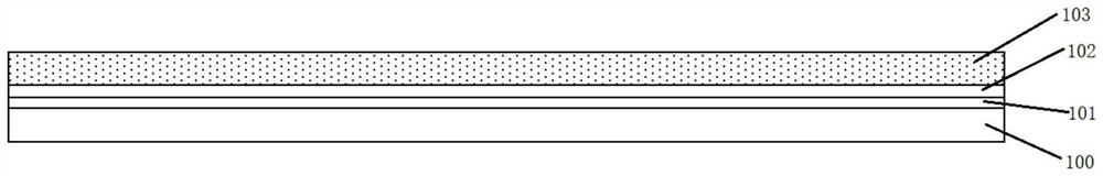
[0027] A first temporary substrate is provided, followed by forming a peelable adhesive layer on the first temporary substrate.

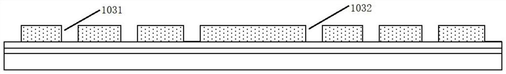
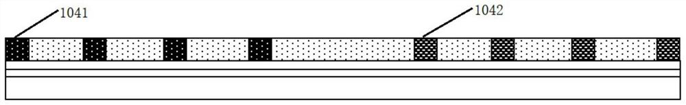
[0028] A first inorganic sacrificial material layer is formed on the peelable adhesive layer, then a first flexible encapsulation layer is formed on the first inorganic sacrificial material layer, and a first antenna structure is formed in the first flexible encapsulation layer and the second ante...


PUM


Abstract

The invention relates to a multi-chip package with an antenna structure and a preparation method thereof. The first antenna structure, the second antenna structure, the third antenna structure and the fourth antenna structure are formed in the first preset antenna pattern, the second preset antenna pattern, the third preset antenna pattern and the fourth preset antenna pattern in a spin-coating mode of the metal nanowire solution, through the preparation process, the connection tightness of the antenna structures and the flexible resin packaging layer can be improved conveniently, and then stripping and falling of the antenna structures can be avoided. Furthermore, the first antenna structure and the third antenna structure are stacked, and the second antenna structure and the fourth antenna structure are stacked, so that the signal transmitting strength of the antenna structure or the signal receiving capability of the antenna structure is effectively improved. Meanwhile, due to the arrangement of the first isolation structure and the second isolation structure, interference between the antenna structures, between the semiconductor chips and between redistribution lines can be effectively avoided, and then the function stability of multi-chip packaging is guaranteed.

Description

technical field [0001] The invention relates to the field of semiconductor packaging, in particular to a multi-chip package with an antenna structure and a preparation method thereof. Background technique [0002] In the preparation process of the existing package structure with antenna, it is usually necessary to directly arrange a semiconductor chip on the circuit substrate. Conventionally, the semiconductor chip is connected to the circuit substrate through a wire bonding process or a flip-chip process. electrical connection, and then a plastic encapsulation resin layer is arranged on the semiconductor chip, and then an antenna structure is arranged on the plastic encapsulation resin layer. The above preparation process may easily lead to an unstable antenna structure, which is prone to peeling and falling off. And when a multi-chip packaging structure is involved, each chip needs to be provided with a corresponding antenna structure, and adjacent antenna structures are l...

Claims


Application Information

Patent Timeline
Patent Type & Authority Applications(China)
IPC IPC(8): H01L21/50H01L21/56H01L21/683H01L23/66H01L23/31H01Q1/38H01Q1/52
CPCH01L21/50H01L21/561H01L21/568H01L21/6835H01L23/66H01L23/3107H01Q1/521H01Q1/38H01L2223/6677H01L2221/68359
Inventor 张琳王训朋庄乾勇
Owner WEIHAI IDEACODS ELECTRONICS TECH CO LTD
Why Eureka
Try Eureka