Monolithic heterogeneous integrated structure of top-layer p-type diamond MOSFET and GaN HEMT and preparation method of monolithic heterogeneous integrated structure

A diamond and diamond layer technology, which is applied in semiconductor/solid-state device manufacturing, semiconductor/solid-state device components, semiconductor devices, etc., can solve problems such as electrical performance degradation, failure, and heat dissipation performance that cannot meet the application of GaN effect transistors. The effect of junction temperature

Pending Publication Date: 2022-05-27
XIDIAN UNIV
View PDF0 Cites 0 Cited by
  • Summary
  • Abstract
  • Description
  • Claims
  • Application Information

AI Technical Summary

Problems solved by technology

Among them, even if the SiC substrate with high thermal conductivity is used, its heat dissipation performance is far from meeting the application of GaN effect tubes in the microwave high-power field.
In addition, the current maximum operating temperature of silicon-based MOSFET devic

Method used


Image

  • Monolithic heterogeneous integrated structure of top-layer p-type diamond MOSFET and GaN HEMT and preparation method of monolithic heterogeneous integrated structure
  • Monolithic heterogeneous integrated structure of top-layer p-type diamond MOSFET and GaN HEMT and preparation method of monolithic heterogeneous integrated structure
  • Monolithic heterogeneous integrated structure of top-layer p-type diamond MOSFET and GaN HEMT and preparation method of monolithic heterogeneous integrated structure

Examples


Embodiment Construction

[0037] The present invention will be described in further detail below with reference to specific embodiments, but the embodiments of the present invention are not limited thereto.

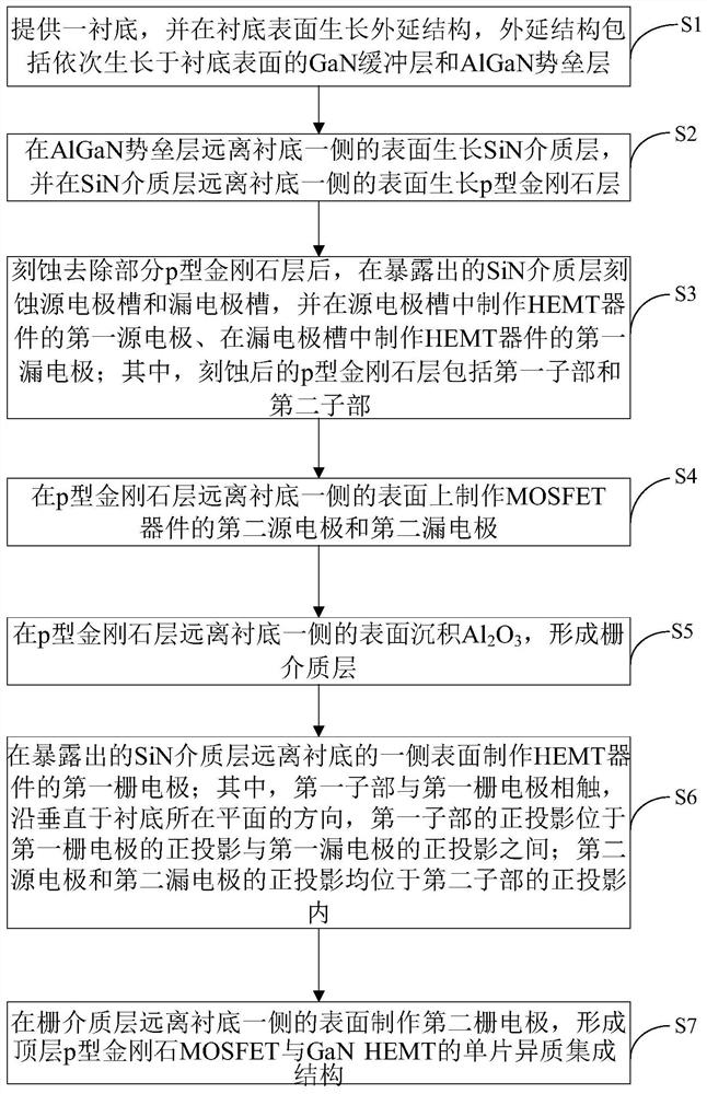
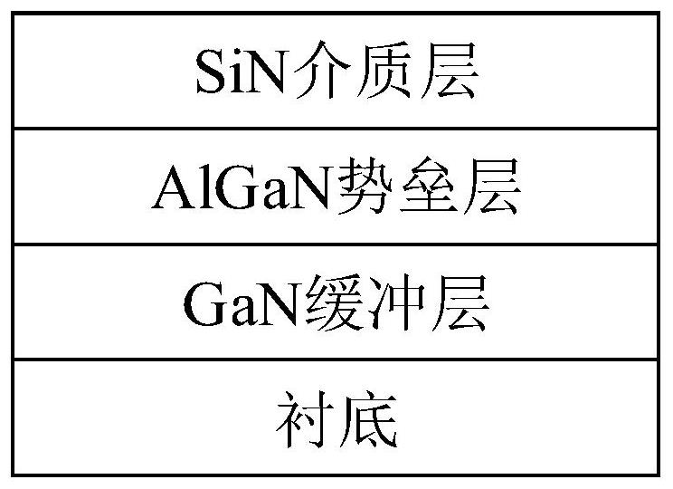
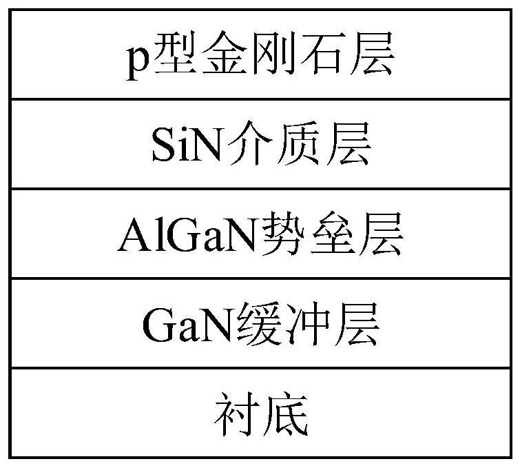
[0038] figure 1 It is a flow chart of the preparation method of the monolithic hetero-integrated structure of the top p-type diamond MOSFET and GaN HEMT provided by the embodiment of the present invention, Figure 2-9 It is a schematic diagram of the preparation method of the monolithic hetero-integrated structure of the top layer p-type diamond MOSFET and GaN HEMT provided by the embodiment of the present invention. See Figure 1-9 , an embodiment of the present invention provides a method for preparing a monolithic hetero-integrated structure of a top p-type diamond MOSFET and a GaN HEMT, including:

[0039] S1, providing a substrate, and growing an epitaxial structure on the surface of the substrate, the epitaxial structure including a GaN buffer layer and an AlGaN barrier layer sequentially ...


PUM

PropertyMeasurementUnit
Thicknessaaaaaaaaaa
Thicknessaaaaaaaaaa

Abstract

The invention discloses a top-layer p-type diamond MOSFET and GaN HEMT monolithic heterogeneous integrated structure and a preparation method thereof, and the method comprises the steps: providing an epitaxial product, and sequentially growing a SiN dielectric layer and a p-type diamond layer on the surface of one side, far away from a substrate, of an AlGaN barrier layer; after part of the p-type diamond layer is removed through etching, a source electrode groove and a drain electrode groove are etched in the SiN dielectric layer, and a first source electrode and a first drain electrode of the HMET device are manufactured; manufacturing a second source electrode and a second drain electrode of the MOSFET device on the surface of the p-type diamond layer; depositing Al2O3 on the surface of the p-type diamond layer to form a gate dielectric layer; and manufacturing a second gate electrode on the surface of the gate dielectric layer to form a monolithic heterogeneous integrated structure of the top p-type diamond MOSFET and the GaN HEMT. The size of the device is reduced, and the integration level of the device is improved; and meanwhile, the heat generation distribution of the GaN HEMTs is modulated, and the heat dissipation capability of the device is improved.

Description

technical field [0001] The invention belongs to the technical field of semiconductors, and in particular relates to a top layer p-type diamond MOSFET and a GaN HEMT monolithic hetero-integrated structure and a preparation method thereof. Background technique [0002] In recent years, due to the advantages of the third-generation semiconductor material GaN, such as wide band gap, high breakdown electric field and high electron saturation velocity, it has unique advantages in high-frequency and high-power fields such as military, aerospace, and communications. However, when the ultra-high integration of semiconductor devices and GaN-based devices are used in high-frequency fields, the accompanying high heat generation phenomenon cannot be ignored. In severe cases, the device may fail. [0003] The thermal conductivity of GaN itself is only 130 W / (m·K) (W / m·Kelvin). Currently, the commonly used substrates for GaN HEMTs mainly include SiC substrates, Si substrates, and sapphire...

Claims


Application Information

Patent Timeline
IPC IPC(8): H01L21/8258H01L23/373H01L27/088
CPCH01L21/8258H01L27/088H01L23/3732
Inventor 杨凌武玫李仕明侯斌王平吕玲张濛马晓华郝跃
Owner XIDIAN UNIV
Why Eureka
Try Eureka