Image sensor and forming method thereof

An image sensor and patterning technology, applied in semiconductor devices, electric solid state devices, radiation control devices, etc., to achieve the effect of improving upper defects, improving performance, and reducing white noise

Pending Publication Date: 2022-06-03
HUA HONG SEMICON WUXI LTD +1
View PDF0 Cites 0 Cited by
  • Summary
  • Abstract
  • Description
  • Claims
  • Application Information

AI Technical Summary

Problems solved by technology

[0004] However, there are still many problems in the formation process of the prior art CMOS image sensor

Method used


Image

  • Image sensor and forming method thereof
  • Image sensor and forming method thereof
  • Image sensor and forming method thereof

Examples


Embodiment Construction

[0032] As described in the background art, there are still many problems in the formation process of the prior art CMOS image sensor. The following will be described in detail with reference to the accompanying drawings.

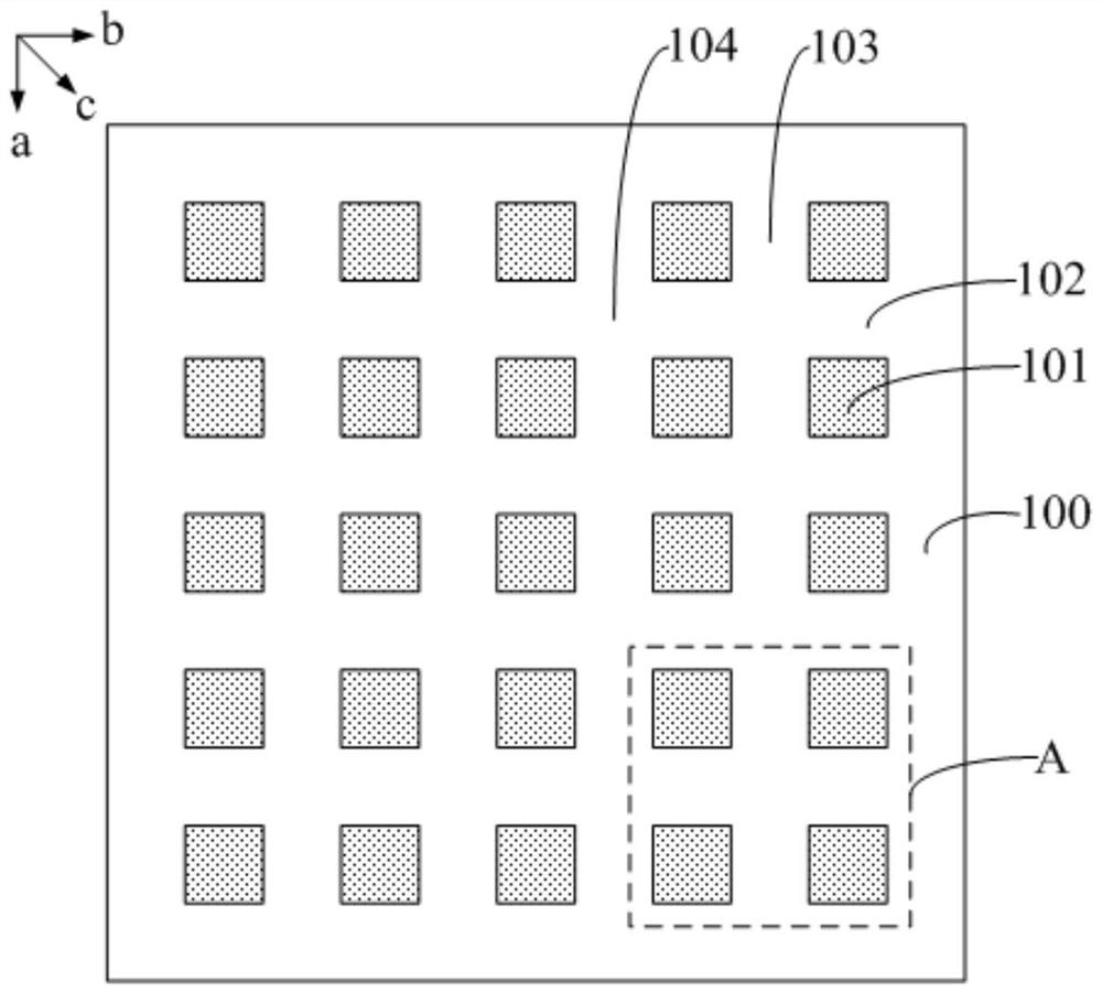
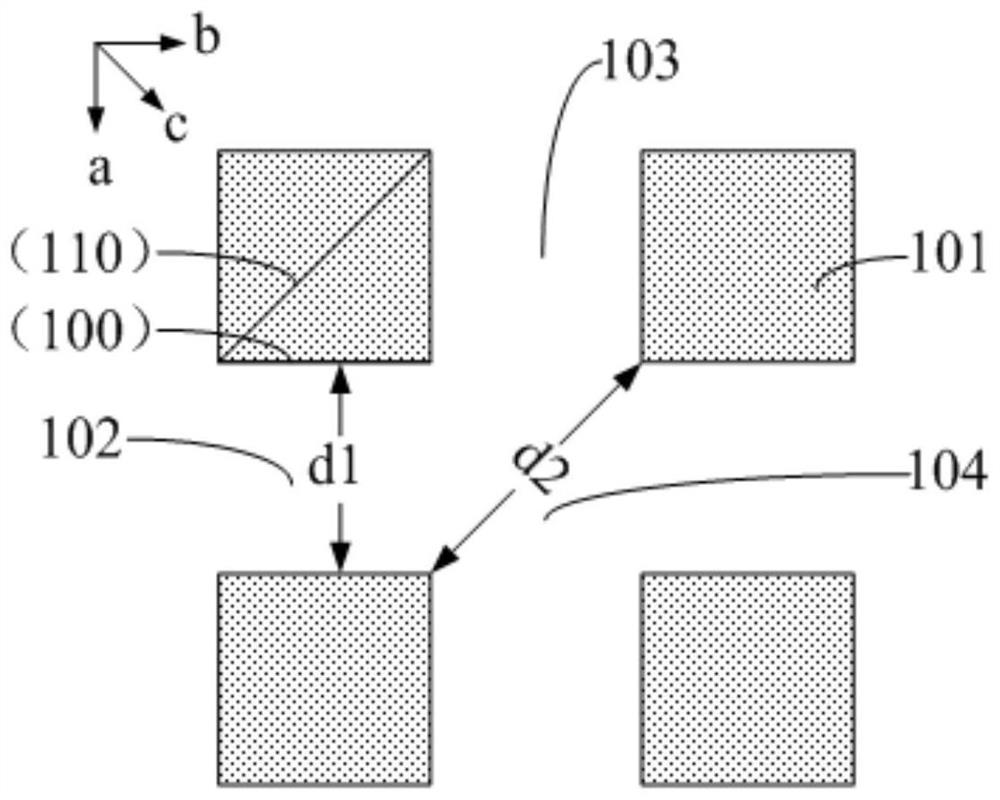
[0033] Figure 1 to Figure 4 It is a schematic structural diagram of each step of a method for forming an image sensor; Figure 5 It is a schematic diagram of the formation process of the doped epitaxial layer of the image sensor.

[0034] Please refer to figure 1 and figure 2 , figure 2 Yes figure 1 In the enlarged schematic diagram of the structure of part A, a substrate 100 is provided, and the substrate 100 has first ions; the substrate 100 is patterned to form a plurality of columnar structures 101 distributed in an array, which are arranged in a row along the first direction a There are first deep trenches 102 between the columnar structures 101 of the cloth, second deep trenches 103 are arranged between the columnar structures 101 arranged al...


PUM


Abstract

The invention discloses an image sensor and a forming method thereof. The method comprises the following steps: providing a substrate; patterning the substrate to form a plurality of columnar structures distributed in an array mode, first deep grooves are formed among the columnar structures arranged in the first direction, second deep grooves are formed among the columnar structures arranged in the second direction, and crossed deep grooves are formed among the columnar structures arranged in the third direction, the side wall, perpendicular to the first direction, of the columnar structure is a (110) crystal face, and the diagonal plane, perpendicular to the third direction, of the columnar structure is a (100) crystal face; and forming doped epitaxial layers in the first deep trench, the second deep trench and the crossed deep trench. Through the arrangement that the side wall, perpendicular to the first direction, of the columnar structure is the (110) crystal face, and the diagonal plane, perpendicular to the third direction, of the columnar structure is the (100) crystal face, the defect generated when the crossed deep grooves are filled with the final seal can be obviously overcome, white noise is effectively reduced, and the performance of the finally formed image sensor is improved.

Description

technical field [0001] The present invention relates to the technical field of semiconductor manufacturing, and in particular, to an image sensor and a method for forming the same. Background technique [0002] Image sensors are semiconductor devices that convert optical images into electrical signals. Because of the advantages of low power consumption and high signal-to-noise ratio, CMOS image sensors (CMOS Image Sensor, CIS) have been widely used in various fields. [0003] The most commonly used Pixel unit in a CMOS image sensor contains a photodiode PD and four MOS transistors, including a transfer transistor TX, a reset transistor RST, a source follower transistor SF, a row select transistor RS, and a floating diffusion region FD, which can realize the photoelectric Control of selection, reset, signal output, signal amplification and readout of diode PD. The principle is that when light illuminates the photodiode PD, the photodiode PD will generate the accumulation of ...

Claims


Application Information

Patent Timeline
Patent Type & Authority Applications(China)
IPC IPC(8): H01L27/146
CPCH01L27/14687H01L27/14632H01L27/14692H01L27/14643H01L27/1463H01L27/14689H01L27/1461H01L27/14607Y02P70/50H01L31/035281H01L31/036H01L31/1804
Inventor 李佳龙房子荃范晓王函陈广龙钱文生
Owner HUA HONG SEMICON WUXI LTD
Why Eureka
Try Eureka