Quantum dot light emitting diode and preparation method thereof

A quantum dot light-emitting and diode technology, which is applied in semiconductor/solid-state device manufacturing, semiconductor devices, electrical components, etc., can solve the problems of device efficiency that needs to be improved, achieve balance improvement, improve luminous efficiency, and improve hole transport efficiency Effect

Pending Publication Date: 2022-06-03
TCL CORPORATION
View PDF0 Cites 0 Cited by
  • Summary
  • Abstract
  • Description
  • Claims
  • Application Information

AI Technical Summary

Problems solved by technology

[0005] In view of the above deficiencies in the prior art, the purpose of the present invention is to provide a quantum dot light-emitting diode and its preparation method, aiming to solve the problem that the efficiency of existing devices still needs to be improved

Method used


Image

  • Quantum dot light emitting diode and preparation method thereof
  • Quantum dot light emitting diode and preparation method thereof

Examples


Embodiment 1

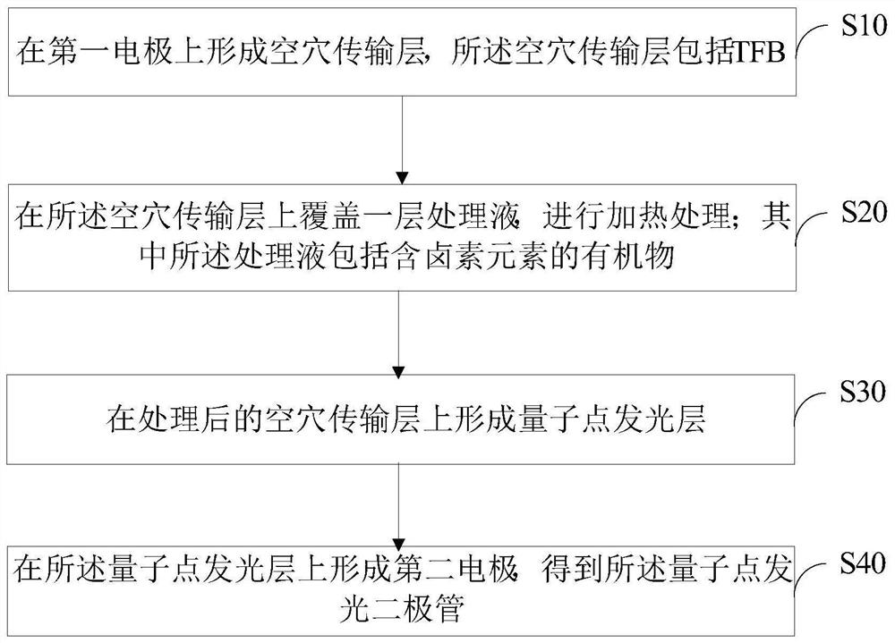
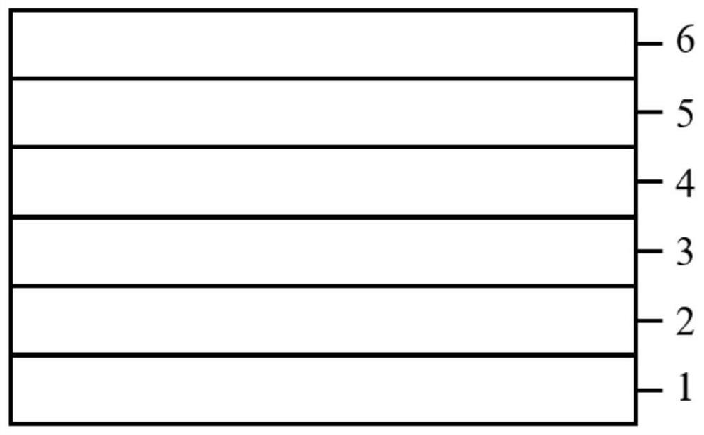
[0051] Evaporate ITO on the substrate as the first electrode, the thickness of ITO is 40nm, then UVO (ultraviolet light ozone) cleaning for 15min, cleaning the surface while improving the surface wettability, and improve the work function of ITO;

[0052] A layer of PEDOT:PSS was spin-coated on ITO as a hole injection layer. The spin-coating speed was 4000 rpm for 40 s, and then annealed at 150 °C for 15 min. The whole step was carried out in air;

[0053] A layer of TFB was spin-coated on the hole injection layer as a hole transport layer. The TFB was dissolved in chlorobenzene at a concentration of 8 mg / ml. 20min, the whole step is carried out in the glove box;

[0054] Treat the surface of the TFB layer, drop an ethanol solution of trifluoromethoxybenzene on the surface of the TFB layer, the concentration of trifluoromethoxybenzene is 1 mg / ml, and then heat at 120 ° C for 10 min;

[0055] The quantum dot light-emitting layer was spin-coated on the hole transport layer, the...

Embodiment 2

[0059] Evaporate ITO on the substrate as the first electrode, the thickness of ITO is 40nm, then UVO (ultraviolet light ozone) cleaning for 15min, cleaning the surface while improving the surface wettability, and improve the work function of ITO;

[0060] A layer of PEDOT:PSS was spin-coated on ITO as a hole injection layer. The spin-coating speed was 4000 rpm for 40 s, and then annealed at 150 °C for 15 min. The whole step was carried out in air;

[0061] A layer of TFB was spin-coated on the hole injection layer as a hole transport layer. The TFB was dissolved in chlorobenzene at a concentration of 8 mg / ml. 20min, the whole step is carried out in the glove box;

[0062] Treat the surface of the TFB layer, drop a trichloromethylphenol ethanol solution on the surface of the TFB layer, the solution concentration is 0.5 mg / ml, and then heat at 100 ° C for 20 min;

[0063] The quantum dot light-emitting layer was spin-coated on the hole transport layer, the quantum dots were dis...


PUM

PropertyMeasurementUnit
thicknessaaaaaaaaaa
thicknessaaaaaaaaaa
thicknessaaaaaaaaaa

Abstract

The invention discloses a quantum dot light emitting diode and a preparation method thereof. The preparation method comprises the following steps: forming a hole transport layer on an anode, wherein the hole transport layer comprises a TFB; covering the hole transport layer with a layer of treatment liquid, and carrying out heating treatment; wherein the treatment liquid comprises a halogen element-containing compound; forming a quantum dot light-emitting layer on the processed hole transport layer; and forming a cathode on the quantum dot light-emitting layer to obtain the quantum dot light-emitting diode. The surface of the TFB hole transport layer is post-processed by using the halogen element-containing compound, and due to the existence of halogen, the HOMO energy level of the TFB can be reduced, so that the interface potential barrier between the TFB and the quantum dots is reduced, the transmission capability of holes from the TFB to the quantum dots is improved, the overall hole transport efficiency of the device is improved, and the luminous efficiency of the device is improved; meanwhile, damage to a functional layer in the device is reduced, and the service life of the device is prolonged.

Description

technical field [0001] The invention relates to the field of quantum dot light-emitting devices, in particular to a quantum dot light-emitting diode and a preparation method thereof. Background technique [0002] Quantum dot electroluminescence display technology has become the best candidate for next-generation display technology due to its tunable wavelength, high color saturation, high material stability, and low fabrication cost. After nearly two decades of development, the external quantum efficiency of quantum dot light-emitting diodes has increased from 0.01% to over 20%. In terms of device efficiency, quantum dot light-emitting diodes (QLEDs) are quite close to organic light-emitting diodes (OLEDs). However, despite the above-mentioned advantages of quantum dot devices, the performance of current devices has not fully met the requirements of industrialization, especially for blue QLED devices. [0003] At present, the device structure of QLED is similar to that of O...

Claims


Application Information

Patent Timeline
Patent Type & Authority Applications(China)
IPC IPC(8): H01L51/56H01L51/50
CPCH10K71/12H10K50/11H10K2101/40H10K50/155H10K50/00H10K71/00
Inventor 马兴远徐威张建新
Owner TCL CORPORATION
Why Eureka
Try Eureka