Method for representing real space characteristics of two-dimensional polariton

A polariton, real-space technology, applied in the direction of testing semiconductor impurities, instruments, measuring devices, etc., can solve difficult to explain, complex relationship between optical density of states and polariton eigenmodes, and increase the complexity of equipment. and the difficulty of the experiment to overcome the complexity of the measurement

Pending Publication Date: 2022-06-07
NANJING UNIV
View PDF1 Cites 0 Cited by
  • Summary
  • Abstract
  • Description
  • Claims
  • Application Information

AI Technical Summary

Problems solved by technology

However, there are still some defects and deficiencies in the existing technologies: firstly, these technologies are all about the optical local density of states in the detection mode, and the relationship between the optical density of states and the polariton eigenmodes is very complicated and difficult to explain clearly; Secondly, these techniques require the experimental conditions to be in a vacuum, which increases the complexity of the equipment and the difficulty of the experiment.

Method used


Image

  • Method for representing real space characteristics of two-dimensional polariton
  • Method for representing real space characteristics of two-dimensional polariton
  • Method for representing real space characteristics of two-dimensional polariton

Examples


Embodiment Construction

[0024] Objects and functions of the present invention and methods for achieving them are elucidated by referring to the exemplary embodiments.

[0025] The present invention will be further described below with reference to the accompanying drawings and embodiments.

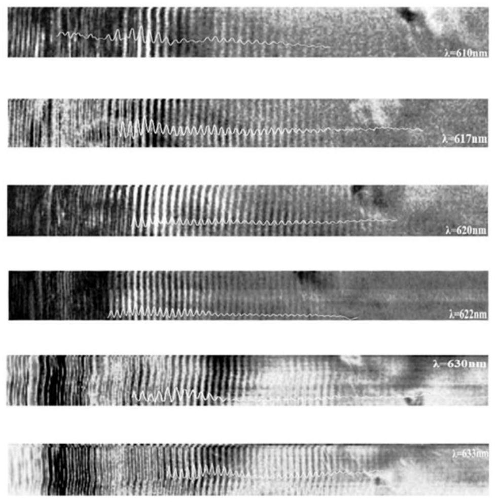
[0026] Taking the heterojunction composed of van der Waals semiconductor layered material WS2 thin film and single crystal silver disk as an example, the method of the present invention is used to characterize its spatial characteristics. The heterojunction has a lateral dimension of 70 microns and a longitudinal thickness of 2 microns.

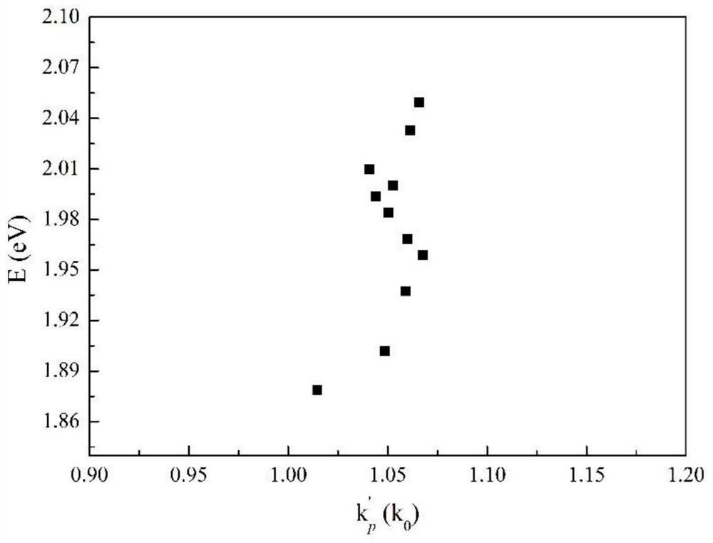
[0027] refer to Figure 1-Figure 4 , the present invention provides a method for characterizing the real space characteristics of two-dimensional polaritons, the steps are as follows:

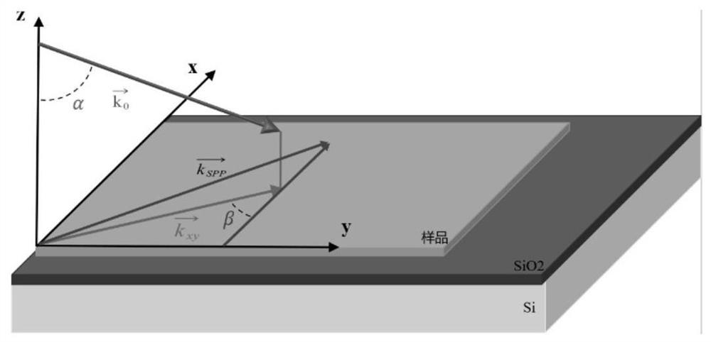
[0028] figure 1 It is a schematic structural diagram of the experimental measurement in the present invention. like figure 1 , the cantilever of a scattering-type scanning near-field optical...


PUM

PropertyMeasurementUnit
sizeaaaaaaaaaa
thicknessaaaaaaaaaa
sizeaaaaaaaaaa

Abstract

The invention provides a method for representing real space characteristics of two-dimensional polaritons, which comprises the following steps of: S1, placing a sample to be tested on a SiO2 / Si substrate, and enabling one edge of the sample to be tested and the edge of a cantilever arm of a scattering type near-field optical microscope to form an angle of 45 degrees; s2, enabling the needle point of the scattering type near-field optical microscope to scan along the edge vertical to the tested sample, sequentially changing the wavelength of the excitation laser light source, and scanning by the scattering type near-field optical microscope to obtain a near-field real space image; s3, Fourier transform processing is carried out on the near-field real space images obtained in the step 2 one by one, and a wave vector real part k'p and a propagation length Lp of a hybrid polariton mode are obtained respectively; and S4, obtaining wave vectors k'p and Lp of the hybrid polaritons under each wavelength according to a formula. The diffraction limit is broken through through the scattering type near-field optical microscope, the physical phenomenon of interaction between light and substances in a near-field area is explored, and the real space characteristics of two-dimensional polaritons are presented.

Description

technical field [0001] The invention relates to the technical field of nano-optical imaging for near-field optical detection, in particular to a scattering-type near-field optical microscope to characterize a van der Waals semiconductor layered material with nanometer thickness or a two-dimensional hybrid formed by a heterojunction formed by a van der Waals semiconductor layered material and a metal. A method for real-space characterization of 3D polaritons. Background technique [0002] Optical imaging plays an important role in modern science. However, the spatial resolution of traditional optical imaging technology is limited by the diffraction limit, which cannot solve the research of optical phenomena at the nanometer scale, but can break through the near field of traditional optical diffraction limit. Optical imaging technology can solve this problem. [0003] The spatial resolution of near-field optical imaging is determined by the distance between the sample and the...

Claims


Application Information

Patent Timeline
Patent Type & Authority Applications(China)
IPC IPC(8): G01N21/84G01Q60/18
CPCG01N21/84G01Q60/18G01N2021/8461
Inventor 杨慧秦康左宗岩董子豪张学进
Owner NANJING UNIV
Why Eureka
Try Eureka