Electrically controllable monomolecular switching device and preparation method thereof
A technology for switching devices and molecular devices, applied in the field of electrically controllable single-molecule switching devices and their preparation, can solve the problems of increased energy consumption, difficult integrated application, and difficult switching control of integrated circuits, and achieves the effect of stable electrical control.
- Summary
- Abstract
- Description
- Claims
- Application Information
AI Technical Summary
Problems solved by technology
Method used
Image
Examples
Embodiment 1
[0104] This embodiment is a single-molecule switching device with a liquid gate.
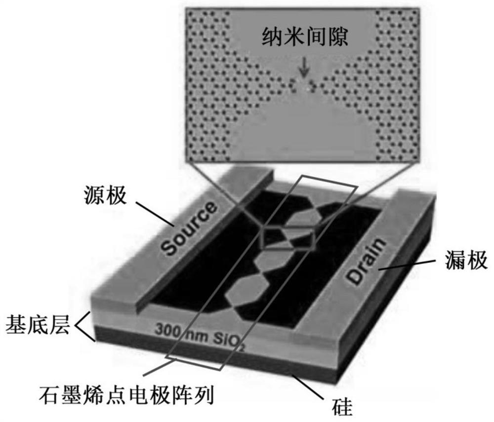
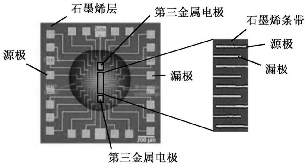
[0105] like Figure 2a As shown, the single-molecule switching device is a graphene-based single-molecule device, and the single-molecule switching device is fabricated into a chip, which is based on SiO 2 / Si wafer substrates can be called electrically controllable single-molecule transistor switching devices. Including: basal layer ( Figure 2a not shown) and graphene layers. A graphene layer is located on the base layer. The graphene layer is plated with at least a pair of metal electrodes arranged oppositely. In each pair of metal electrodes, one is used as the source electrode of the triode, and the other is used as the drain electrode of the triode. The graphene between each pair of source and drain forms a conductive channel. In addition, a third metal electrode is also arranged on the graphene layer.
[0106] like Figure 2a As shown, multiple pairs of source and drain, and graphe...
Embodiment 2
[0121] This embodiment is a single-molecule switching device with a solid-state gate.
[0122] like Figure 4a As shown, the single-molecule switching device is a graphene-based single-molecule device, and the single-molecule switching device is fabricated into a chip, which is based on SiO 2 / Si wafer substrate. Including: basal layer ( Figure 4a not shown) and graphene layers. A graphene layer is located on the base layer. The graphene layer is plated with at least a pair of metal electrodes arranged oppositely. In each pair of metal electrodes, one is used as the source electrode of the triode, and the other is used as the drain electrode of the triode. The graphene between each pair of source and drain forms a conductive channel.
[0123] like Figure 4a As shown, multiple pairs of source and drain, and graphene between each pair of source and drain form a graphene strip in the middle of the chip.
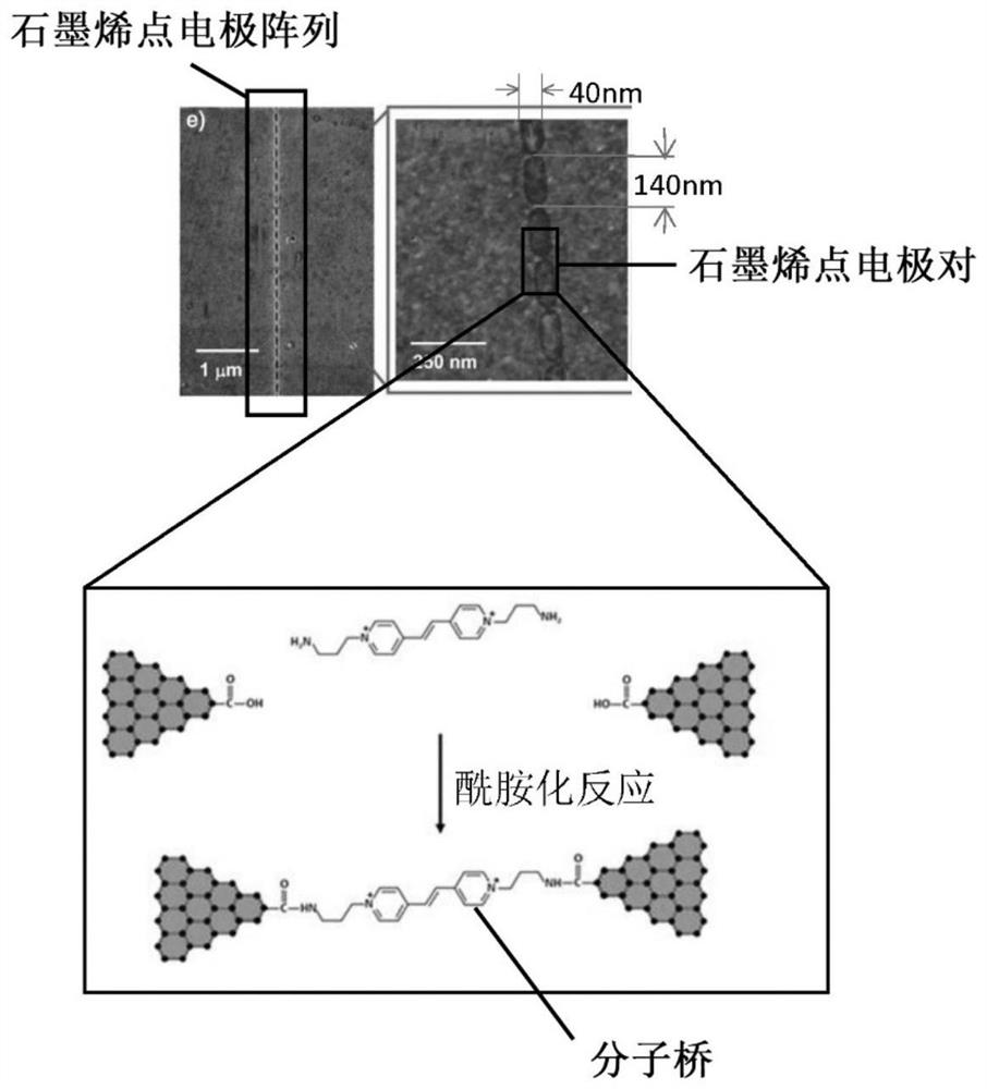
[0124] The structure of the graphene point electrode in the single...
PUM
| Property | Measurement | Unit |
|---|---|---|
| Width | aaaaa | aaaaa |
| Length | aaaaa | aaaaa |
Abstract
Description
Claims
Application Information


