Power amplifier

A power amplifier, temperature sensor technology, applied in amplifiers, RF amplifiers, amplifier types, etc., can solve problems such as violation of high output

Pending Publication Date: 2022-06-21
MURATA MFG CO LTD
View PDF1 Cites 0 Cited by
  • Summary
  • Abstract
  • Description
  • Claims
  • Application Information

AI Technical Summary

Problems solved by technology

Conversely, if feedback control is performed so that the transistor does not break down at low temperatures, the output will be suppressed at high temperatures even though there is still a margin to the breakdown upper limit voltage, which violates high output.

Method used


Image

  • Power amplifier
  • Power amplifier
  • Power amplifier

Examples


no. 1 example

[0047] refer to Figure 1 to Figure 10 With the accompanying drawings, the power amplifier of the first embodiment will be described.

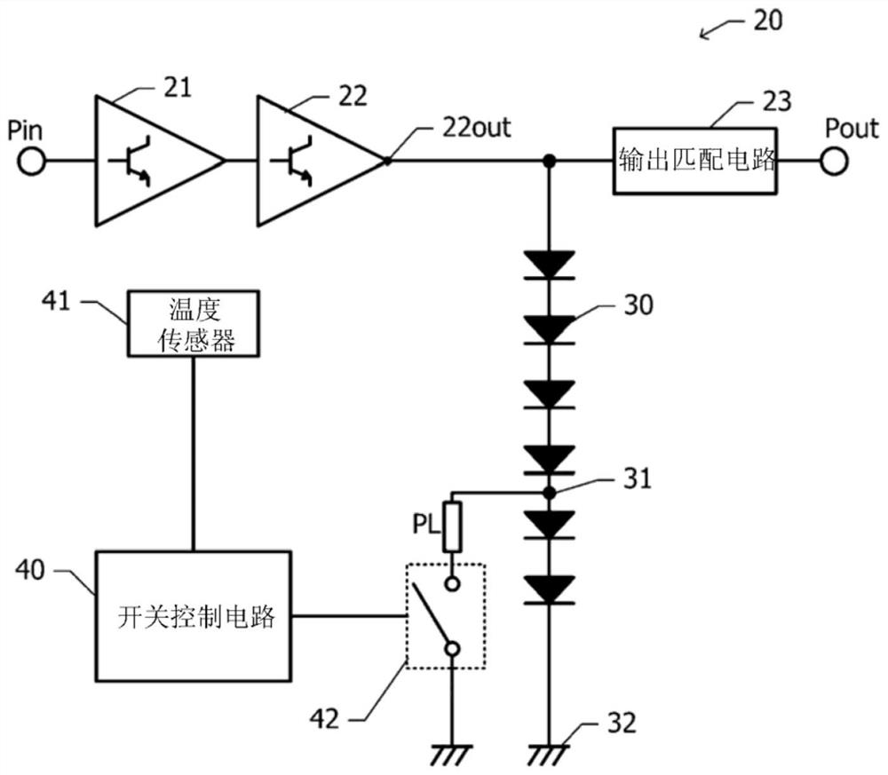
[0048] figure 1 is a block diagram of the power amplifier of the first embodiment. The power amplifier of the first embodiment is composed of two stages of a driver-stage amplifying circuit 21 and a power-stage amplifying circuit 22 . The high-frequency signal input from the input terminal Pin is amplified in the driver stage amplifier circuit 21 , and the amplified high-frequency signal is further amplified in the power stage amplifier circuit 22 .

[0049] The high-frequency signal amplified in the power stage amplifier circuit 22 and output from the output port 22out is output from the output terminal Pout via the output matching circuit 23 . A plurality of clamp diodes 30 connected in multiple stages are connected between the output port 22out of the power stage amplifier circuit 22 and the ground line 32 . The plurality of clamp diode...

no. 2 example

[0100] Next, refer to Figure 11 as well as Figure 12 The power amplifier of the second embodiment will be described. Below, for and reference Figure 1 to Figure 10 The same configuration of the power amplifier of the first embodiment described in the accompanying drawings is omitted.

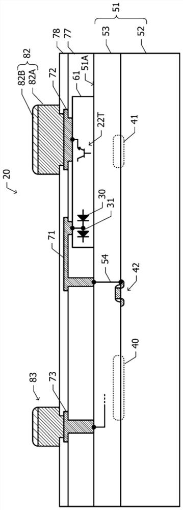
[0101] Figure 11 is a schematic cross-sectional view of the power amplifier 20 of the second embodiment. Furthermore, in Figure 11 In the figure, a part of the circuit is schematically shown by a circuit diagram symbol and a dotted line. In the first embodiment ( figure 2 ), the lead point 31 of the clamp diode 30 connected in multiple stages and the switch 42 are connected by the inter-component connection wiring 71 in the rewiring layer. On the other hand, in the second embodiment, the lead point 31 of the clamp diode 30 connected in multiple stages and the switch 42 are connected via a path intersecting with the interface of the second member 61 and the first member 51 in surface...

no. 3 example

[0110] Next, refer to Figure 13 The power amplifier of the third embodiment will be described. Below, for and reference Figure 1 to Figure 10 The same configuration of the power amplifier of the first embodiment described in the accompanying drawings is omitted.

[0111] Figure 13 is a block diagram of the power amplifier of the third embodiment. In the first embodiment ( figure 1 ), a clamping diode 30 connected in multiple stages is connected between the output port 22out of the power stage amplifier circuit 22 and the ground wire 32 , and the clamp diode is not connected to the output port of the driver stage amplifier circuit 21 . On the other hand, in the third embodiment, the clamp diode 35 connected in multiple stages is also connected between the output port 21out of the amplifier circuit 21 of the driver stage and the ground line 32 . The number of stages of the clamp diodes 35 connected to the amplifier circuit 21 of the driver stage need not be the same as t...


PUM


Abstract

The invention provides a power amplifier capable of appropriately suppressing output voltage according to temperature. A second member including a semiconductor region of a compound semiconductor system is bonded to a first surface of a first member including the semiconductor region. The second member includes: an amplifier circuit including a semiconductor element of a compound semiconductor system; and a plurality of clamping diodes connected in multiple stages and inserted between the output port of the amplifier circuit and the ground. The first member includes: a switch connected between a lead-out point, which is a midway point of a plurality of clamp diodes connected in multiple stages, and a ground; a temperature sensor; and a switch control circuit that performs on / off control of the switch on the basis of the measurement result of the temperature sensor. The lead-out point and the switch are connected via a path including an inter-member connection wiring composed of a metal pattern disposed on an interlayer insulating film from a first surface of the first member to a surface of the second member, or via a path intersecting an interface at which the first member and the second member are joined.

Description

technical field [0001] The present invention relates to power amplifiers. Background technique [0002] One of the main components mounted on a mobile terminal is a high-frequency power amplifier. In order to increase the wireless transmission capacity of mobile terminals, wireless communication standards using many frequency bands, such as carrier aggregation (CA), have been put into practical use. As the frequency band used increases, the circuit configuration of the RF front end becomes complicated. In addition, the circuit configuration of the RF front end is further complicated in order to be able to use the sub-6 GHz frequency band of the fifth generation mobile communication system (5G). [0003] When the circuit configuration of the RF front end becomes complicated, the loss due to filters, switches, etc. inserted in the transmission line from the high-frequency power amplifier to the antenna increases. As a result, in the high-frequency power amplifier, in additi...

Claims


Application Information

Patent Timeline
Patent Type & Authority Applications(China)
IPC IPC(8): H01L23/34H01L23/528H03F1/30H03F3/195H03F3/213
CPCH01L23/34H01L23/528H03F1/30H03F3/195H03F3/213H03F2200/447H03F1/52H03F3/245H03F2200/441H03F2200/468H03F2200/451H01L23/66
Inventor 筒井孝幸近藤将夫
Owner MURATA MFG CO LTD
Why Eureka
Try Eureka