LED and semiconductor laser chip sorting machine control method and sorting machine

A control method and semiconductor technology, which is applied in the field of mechanical equipment control, can solve the problems of restricting the development of LED and semiconductor laser chip industries, poor sorting accuracy, and slow sorting speed, so as to improve the technical level and mass production capacity. The effect of small area and improved sorting speed

Inactive Publication Date: 2022-06-24
山东泓瑞光电科技有限公司
View PDF0 Cites 5 Cited by
  • Summary
  • Abstract
  • Description
  • Claims
  • Application Information

AI Technical Summary

Problems solved by technology

[0004] The first method is that the test sorting is done by the same equipment. The disadvantage of this method is that the sorting speed is very slow and the production capacity is low;
[0005] The second method is that the testing and sorting are completed by two devices. Although this method speeds up the sorting speed, it has low reliability, is prone to errors, and has poor sorting accuracy;
[0006] It can be seen that the sorting speed and sorting accuracy of LED and semiconductor laser chip production have become the bottleneck problem of LED and semiconductor laser chip production, restricting the development of LED and semiconductor laser chip industry

Method used


Image

  • LED and semiconductor laser chip sorting machine control method and sorting machine
  • LED and semiconductor laser chip sorting machine control method and sorting machine
  • LED and semiconductor laser chip sorting machine control method and sorting machine

Examples


Embodiment 1

[0063] like figure 1 As shown, a control method for an LED and semiconductor laser chip sorting machine includes an initial step, a loading and unloading step of silicon wafers, a loading and unloading step of blanks, and a rapid sorting step of chips. The CCD camera performs image recognition to obtain the precise position information of the chip, and adopts double suction nozzles to pick up and place the chip, so that the sorting of the chip can be realized quickly and accurately.

[0064] Initial steps:

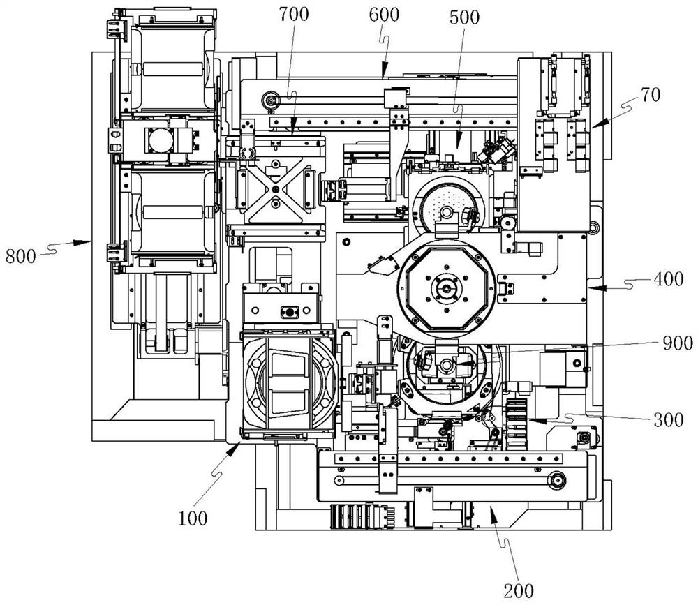
[0065] like figure 1 , image 3 , Figure 16 ,and Figure 22 As shown in common, first, through manual adjustment, the center of the lens of the CCD camera 900 on the side of the wafer table 300, the suction nozzle 407 and the ejector pin 973 of the ejector 950 are adjusted to a straight line in the vertical direction. The center of the lens of the CCD camera 900 on the side of the table 500 and the two points of the suction nozzle 407 are adjusted to a straight line ...

Embodiment 2

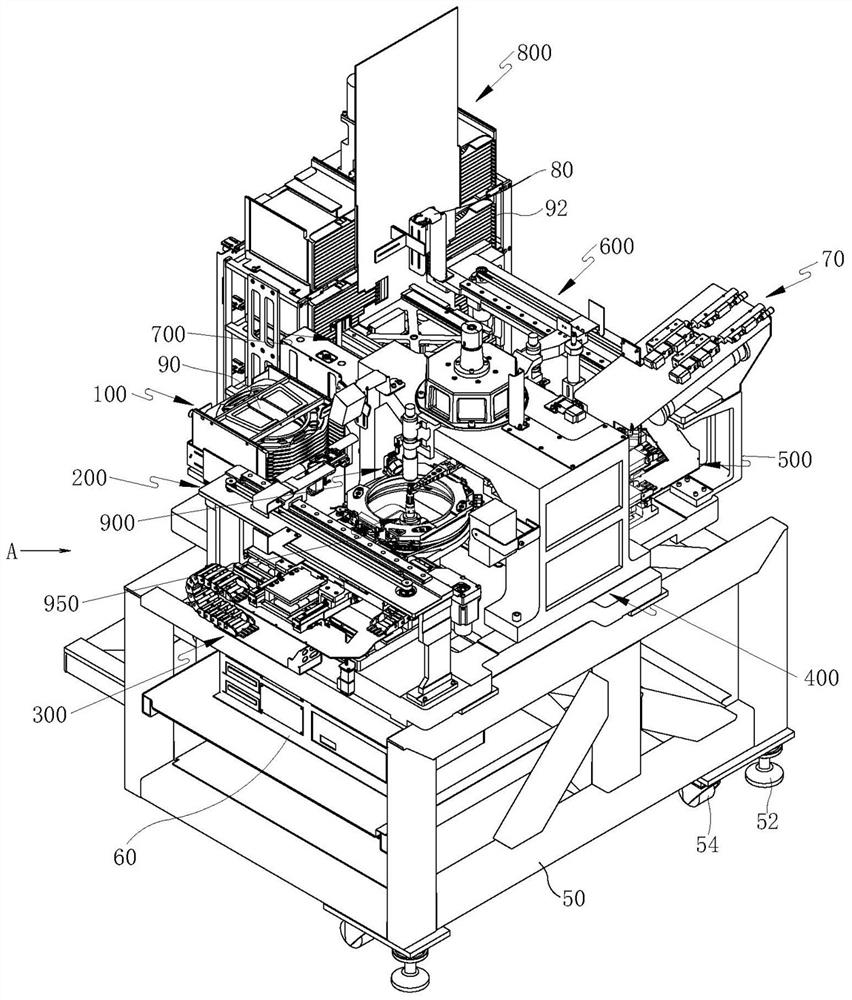
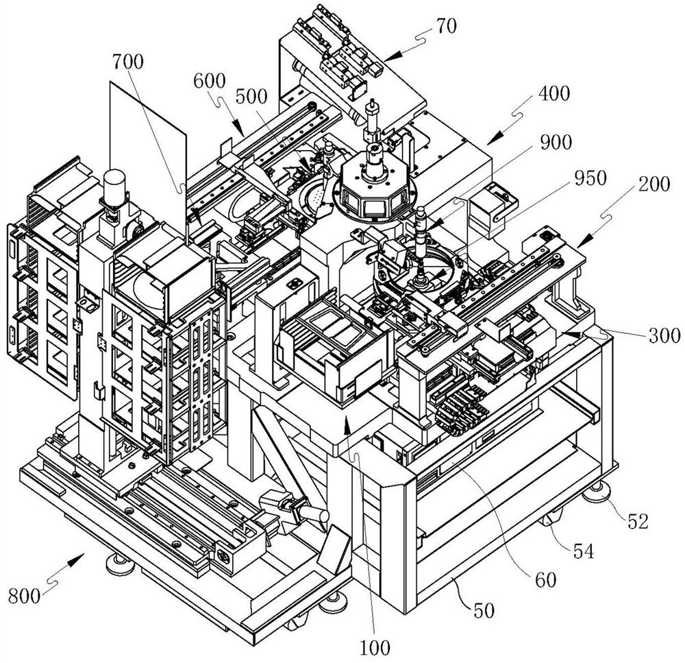
[0087] like figure 1 , figure 2 and image 3 Commonly shown, an LED and semiconductor laser chip sorting machine for implementing the control method for the LED and semiconductor laser chip sorting machine described in the first embodiment includes a rack 50, and a silicon wafer lifting table 100 is installed on the rack 50. , Silicon wafer robot 200, wafer table 300, suction and release device 400, placing table 500, material robot 600, buffer table 700, material lifting bin 800, CCD camera 900 and ejector 950. A control box 60 , an air circuit assembly 70 , a barcode scanner 80 and various positioning and limit sensors are also installed on the rack 50 . The bottom of the frame 50 is provided with supporting feet 52 and universal wheels 54 .

[0088] like figure 1 and Figure 4 As shown in common, the wafer lifting platform 100 includes a wafer cassette bracket 110 and a power box 140 for driving the wafer cassette bracket 110 to ascend and descend, and the wafers carr...


PUM


Abstract

The invention discloses an LED and semiconductor laser chip sorting machine control method and a sorting machine, and relates to the technical field of mechanical equipment control. The method comprises the steps that a silicon wafer lifting table moves, and a silicon wafer to be grabbed is conveyed to a silicon wafer mechanical arm grabbing position; the silicon wafer manipulator grabs the silicon wafer and places the silicon wafer on a silicon wafer workbench; the material sheet lifting bin moves to convey the material sheets to be grabbed to a material sheet manipulator grabbing position; the material sheet manipulator is used for grabbing the material sheet and placing the material sheet on the placing workbench; and the chip is sucked up by a suction nozzle of the suction and release device through recognition of a CCD camera, the suction nozzle of the suction and release device swings to a placement position to place the chip on the material sheet, meanwhile, the other suction nozzle swings to the suction position to suck the next chip, and the process is repeated until the chips of the same grade on the silicon wafer are all placed on the material sheet.

Description

technical field [0001] The invention relates to the technical field of mechanical equipment control, in particular to a control method for an LED and semiconductor laser chip sorting machine and a LED and semiconductor laser chip sorting machine. Background technique [0002] The scale of the LED and semiconductor laser industry is developing very rapidly, and the market potential is huge, but its development cannot be separated from the development of the LED and semiconductor laser equipment industry. And the LED and semiconductor laser industry has its particularity. Due to the production process, each LED and semiconductor laser chip is unique and has slightly different electronic and optical characteristics, which requires all LED and semiconductor laser chips. Laser chips are tested and sorted according to their unique characteristics. However, the sorting of LED and semiconductor laser chips is very difficult. The main reason is that the size of the chips is generall...

Claims


Application Information

Patent Timeline
Patent Type & Authority Applications(China)
IPC IPC(8): B07C5/34B07C5/02B07C5/36
CPCB07C5/34B07C5/02B07C5/362
Inventor 陈国强刘江涛董月宁
Owner 山东泓瑞光电科技有限公司
Why Eureka
Try Eureka