Semiconductor structure and forming method thereof

A semiconductor and optical waveguide technology, applied in the field of semiconductor structure and its formation, can solve problems such as poor performance, achieve good performance, improve light wave transmission efficiency, and reduce the second refractive index

Pending Publication Date: 2022-07-01
SEMICON MFG INT (SHANGHAI) CORP +1
View PDF0 Cites 0 Cited by
  • Summary
  • Abstract
  • Description
  • Claims
  • Application Information

AI Technical Summary

Problems solved by technology

[0005] However, the performance of semiconductor structures formed

Method used


Image

  • Semiconductor structure and forming method thereof
  • Semiconductor structure and forming method thereof
  • Semiconductor structure and forming method thereof

Examples


Embodiment Construction

[0035] It should be noted that the "surface" and "upper" in this specification are used to describe the relative positional relationship in space, and are not limited to whether they are in direct contact.

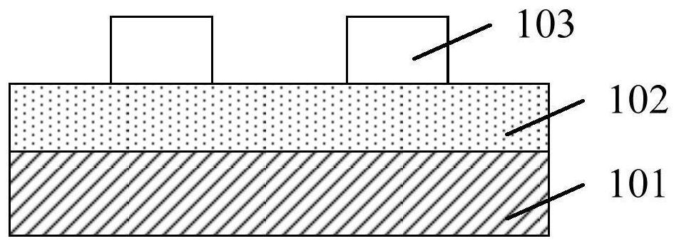
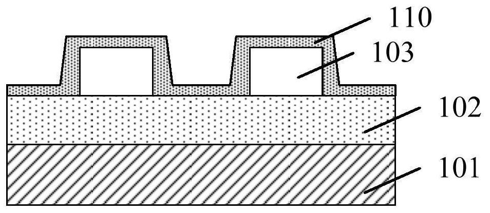
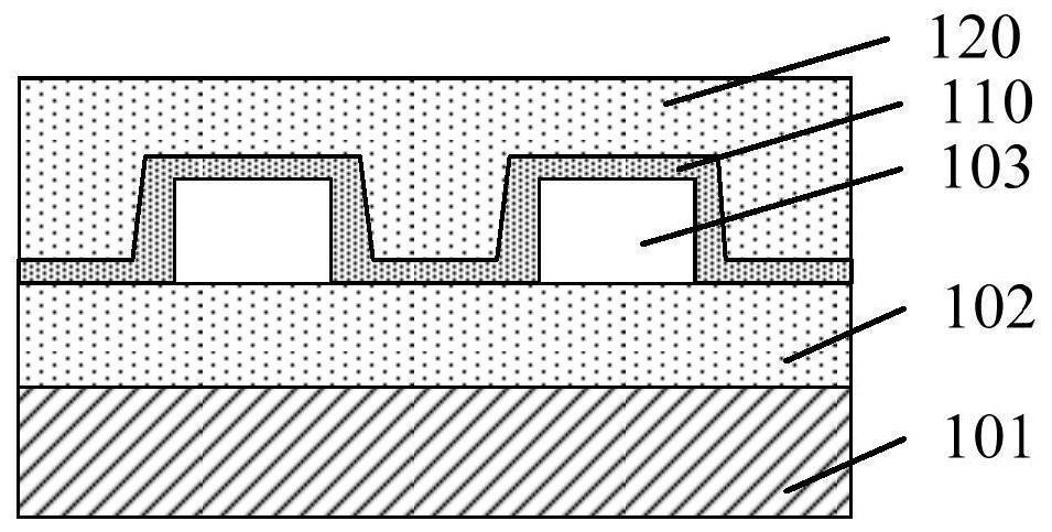
[0036] First, the reasons for the poor performance of the existing semiconductor structure are described in detail with reference to the accompanying drawings. Figure 1 to Figure 3 It is a structural schematic diagram of each step of a method for forming a conventional semiconductor structure.

[0037] Please refer to figure 1 , a substrate 100 is provided, the substrate 100 includes a substrate 101 and an insulating layer 102 located on the surface of the substrate 101 , and an optical waveguide layer 103 is provided on the substrate 100 .

[0038] Please refer to figure 2 , a sidewall layer 110 is formed on the top surface and sidewall surface of the optical waveguide layer 103 and the surface of the substrate 100 .

[0039] Please refer to image 3 , a dielectric ...


PUM


Abstract

The invention discloses a semiconductor structure and a forming method thereof, and the structure comprises a substrate which is provided with an optical waveguide layer; the first dielectric layer is located on the substrate; the cavity is located between the first dielectric layer and the optical waveguide layer, the cavity is located on the surface of the side wall of the optical waveguide layer, and the bottom of the cavity is flush with the bottom of the optical waveguide layer; the second dielectric layer is located on the first dielectric layer and the optical waveguide layer, and the second dielectric layer is located at the top of the cavity and seals the cavity. An optical waveguide layer is arranged on the substrate; the first dielectric layer is located on the substrate; the cavity is located between the first dielectric layer and the optical waveguide layer, the cavity is located on the surface of the side wall of the optical waveguide layer, and the bottom of the cavity is flush with the bottom of the optical waveguide layer; the second dielectric layer is located on the first dielectric layer and the optical waveguide layer, and the second dielectric layer is located at the top of the cavity and seals the cavity. The performance of the semiconductor structure is good.

Description

technical field [0001] The present invention relates to the technical field of semiconductor manufacturing, and in particular, to a semiconductor structure and a method for forming the same. Background technique [0002] Silicon photonics technology is a low-cost, high-speed optical communication technology based on silicon photonics. Based on silicon-based substrate materials, using CMOS technology, combined with integrated circuits and photonic technologies represented by microelectronics, laser beams are used instead of electronic information to transmit data. [0003] The optical wave guide layer is a guide structure composed of an optically transparent medium (such as quartz glass) for transmitting optical frequency electromagnetic waves. The transmission principle of the optical waveguide layer is that on the interface of the medium with different refractive indices, the total reflection of the electromagnetic wave makes the light wave confined to the waveguide and it...

Claims


Application Information

Patent Timeline
IPC IPC(8): G02B6/122G02B6/132
CPCG02B6/122G02B6/132G02B2006/12061G02B6/136G02B6/1223
Inventor 刘俊代洪刚程东向
Owner SEMICON MFG INT (SHANGHAI) CORP
Why Eureka
Try Eureka