Supercharge Your Innovation With Domain-Expert AI Agents!

FLASH application verification system based on FPGA

A verification system and verification board technology, applied in the field of chip application verification, can solve problems such as incompatibility with different models, insufficient FLASH verification items, and lack of versatility, so as to accelerate device maturity, improve coverage, and speed up the debugging process. Effect

Pending Publication Date: 2022-07-01
BEIJING MXTRONICS CORP +1
View PDF0 Cites 2 Cited by
  • Summary
  • Abstract
  • Description
  • Claims
  • Application Information

AI Technical Summary

Problems solved by technology

[0003] At present, there are relatively few domestic manufacturers who design and produce FLASH for aerospace, and the FLASH verification items are not sufficient, and they cannot be compatible with different models. Most of them use verification systems and verification methods to verify the timing matching of FLASH, which is not universal.

Method used


Image

  • FLASH application verification system based on FPGA
  • FLASH application verification system based on FPGA
  • FLASH application verification system based on FPGA

Examples


Embodiment Construction

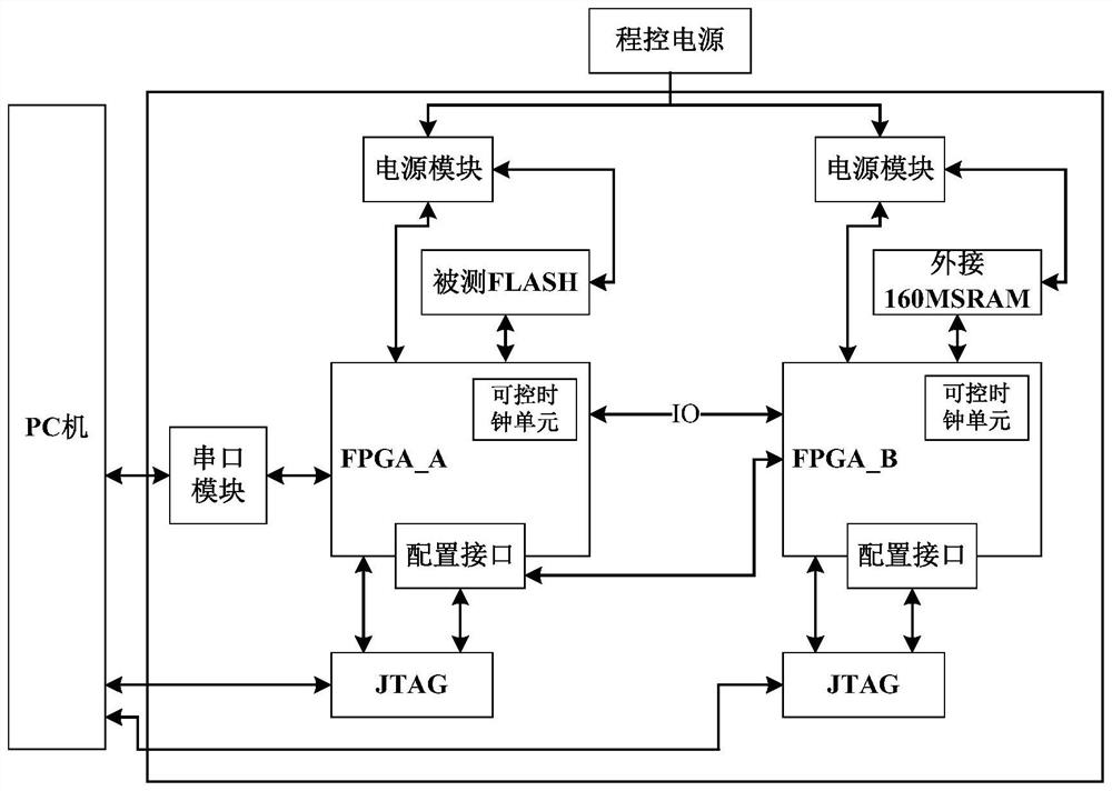
[0046] see figure 1 , the FLASH application verification system of the present invention includes a PC, a FLASH application verification board and a program-controlled power supply.

[0047] The FLASH application verification board includes two FPGAs, serial port modules, power supply modules, configuration memory connectors, JTAG, 160Mb capacity SRAM and FLASH under test.

[0048] The serial port module is used to connect the PC and FPGA_A, send the instructions of the PC to FPGA_A, and feed back the results fed back by FPGA_A to the PC.

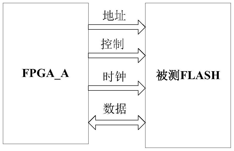
[0049] FPGA_A integrates a FLASH controller and a controllable clock unit. The FLASH controller is connected to the FLASH under test. The FLASH controller receives PC instructions, sends control signals, clocks, addresses and data to the FLASH under test, and collects the output data of the FLASH under test. ; The controllable clock unit is the internal PLL of the FPGA, which is used to generate two clock frequencies, and one is used to main...


PUM


Abstract

The invention discloses a FLASH application verification system based on an FPGA (Field Programmable Gate Array). The FLASH application verification system comprises a PC (Personal Computer), an FPGA application verification board and a FLASH daughter board, the FPGA application verification board is provided with two FPGA chips; each FPGA chip is connected with the FLASH and can independently access the FLASH to carry out verification operation on the FLASH; each FPGA is externally connected with a high-capacity 160 MbSRAM (Static Random Access And the NOR FLASH and the SPI FLASH can be verified by replacing the FLASH daughter board. The invention also discloses a verification method based on the system. The method comprises the following steps: firstly, determining a power-on sequence, carrying out JTAG function verification, carrying out digital logic verification and carrying out read-write function verification. The method is comprehensive in verification function and high in universality, and has important significance on application verification of a series of FLASH.

Description

technical field [0001] The invention belongs to the field of chip application verification, relates to application verification in the field of non-volatile memory, and in particular relates to an FPGA-based FLASH application verification system. Background technique [0002] With the development of science and technology, data storage and processing are becoming more and more important; non-volatile memory, due to its characteristics that data will not be lost when power is turned off, has a wide range of applications. [0003] At present, there are relatively few domestic manufacturers designing and producing FLASH for aerospace, which are not sufficient for FLASH verification projects, and cannot be compatible with different models. Most of the application verification systems and verification methods are mainly used to verify the timing matching of FLASH, which is not universal. To this end, it is necessary to develop a FLASH application verification system, which can be...

Claims


Application Information

Patent Timeline
IPC IPC(8): G06F30/343
CPCG06F30/343
Inventor 王佳陈雷陈茂鑫李建成董方磊许凯亮周涛杨作涵
Owner BEIJING MXTRONICS CORP
Features
  • R&D
  • Intellectual Property
  • Life Sciences
  • Materials
  • Tech Scout
  • Unparalleled Data Quality
  • Higher Quality Content
  • 60% Fewer Hallucinations
Learn More