Method and equipment for creating time delay table of FPGA (Field Programmable Gate Array) circuit and obtaining time delay

A technology of path delay and delay, which is applied in the direction of electrical digital data processing, computer-aided design, special data processing applications, etc., can solve the problems of increased connection line delay and FPGA circuit difficulty in meeting timing constraints, etc.

Pending Publication Date: 2022-07-08
SHANGHAI FUDAN MICROELECTRONICS GROUP
View PDF0 Cites 0 Cited by
  • Summary
  • Abstract
  • Description
  • Claims
  • Application Information

AI Technical Summary

Problems solved by technology

[0003] With the progress of the manufacturing process, the parasitic parameters (such as parasitic capacitance, resistance, and inductance) of the connection lines in the FPGA chip are increasing, and the delay of the connection lines is also increasing, making it difficult for the design of the FPGA circuit to meet the timing constraints.

Method used


Image

  • Method and equipment for creating time delay table of FPGA (Field Programmable Gate Array) circuit and obtaining time delay
  • Method and equipment for creating time delay table of FPGA (Field Programmable Gate Array) circuit and obtaining time delay
  • Method and equipment for creating time delay table of FPGA (Field Programmable Gate Array) circuit and obtaining time delay

Examples


Embodiment Construction

[0041] In order to make the above objects, features and beneficial effects of the embodiments of the present invention more clearly understood, the specific embodiments of the present invention will be described in detail below with reference to the accompanying drawings.

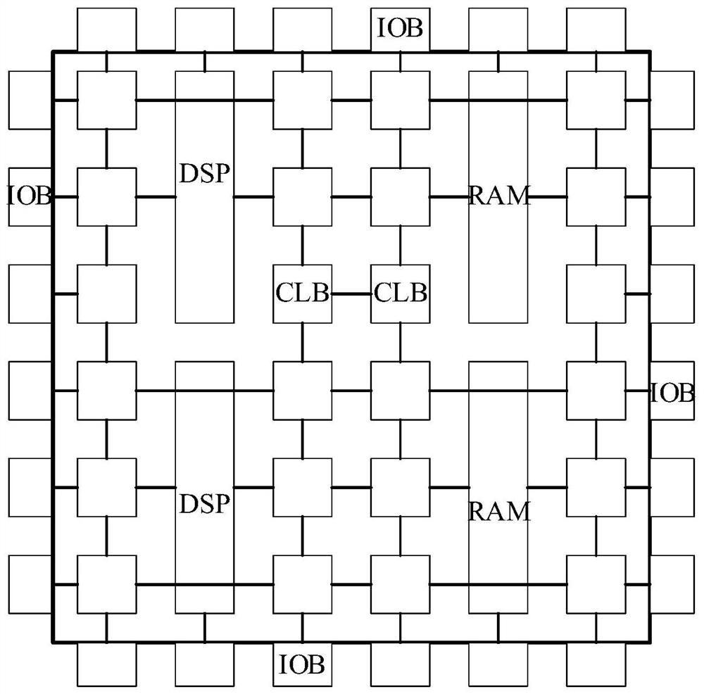
[0042] like figure 1 As shown, the FPGA chip adopts a regular array structure; the center of the array can be taken as the origin, the horizontal right and left directions are the positive and negative directions of the X axis ("X direction"), and the vertical upward and downward directions are respectively The positive and negative directions of the Y-axis ("Y-direction").

[0043] The points in the array may be modules, and the modules include CLB, random access memory (Random Access Memory, RAM), programmable input output block (IOB), digital signal processing module (Digital Signal Processor, DSP) and the like.

[0044] Inside the FPGA chip, the largest number is CLB, which is the most basic module; on...


PUM


Abstract

The embodiment of the invention provides a method for creating a time delay table of an FPGA (Field Programmable Gate Array) circuit and a method and equipment for acquiring time delay, the FPGA circuit comprises a plurality of Slices, the time delay table comprises an internal time delay table, and the method comprises the following steps: determining a plurality of lines from an input pin to an output pin in each Slice in the plurality of Slices; calculating internal time delays from the input pin to the output pin based on the plurality of lines; and storing the input pin and the output pin corresponding to the plurality of lines of each Slice and the corresponding internal time delay between the two pins in an internal time delay table. According to the technical scheme provided by the embodiment of the invention, the estimation of the total time delay can be more accurate, so that the FPGA circuit designed or optimized based on the estimation can meet the time sequence constraint.

Description

technical field [0001] The invention relates to the technical field of integrated circuits, and in particular, to a method and device for creating a delay table of a Field-Programmable Gate Array (FPGA) circuit and acquiring the delay of an FPGA circuit. Background technique [0002] The design process of an FPGA chip mainly includes design input, functional simulation, logic synthesis, technology mapping, logic packaging, layout, routing, timing simulation, bitstream generation and other stages. Among them, the physical implementation stages such as logic packaging, layout, and wiring are very complex. and a critical stage, the results of which directly affect circuit performance, area, reliability, power, and manufacturing yield. [0003] With the advancement of the manufacturing process, the parasitic parameters (such as parasitic capacitance, resistance, and inductance) of the connection lines in the FPGA chip are increasing, and the time delay of the connection lines is...

Claims


Application Information

Patent Timeline
Patent Type & Authority Applications(China)
IPC IPC(8): G06F30/394G06F30/398
CPCG06F30/394G06F30/398
Inventor 王似飞钱港林智锋徐烈伟俞军
Owner SHANGHAI FUDAN MICROELECTRONICS GROUP
Why Eureka
Try Eureka