Organic photoelectric device based on metal-induced organic interface layer and preparation method

A photoelectric device, metal-induced technology, applied in semiconductor/solid-state device manufacturing, semiconductor devices, electric solid-state devices, etc., can solve problems such as poor stability of formally mounted devices, achieve good stability, excellent comprehensive performance, and simple and easy-to-operate manufacturing methods Effect

Pending Publication Date: 2022-07-22
SOUTH CHINA UNIV OF TECH
View PDF0 Cites 1 Cited by
  • Summary
  • Abstract
  • Description
  • Claims
  • Application Information

AI Technical Summary

Problems solved by technology

However, there are few reports on the application of PFN-Br as the cathode interface in flip-chip organic optoelectronic devices, and the stability of front-mounted devices is also poor.

Method used


Image

  • Organic photoelectric device based on metal-induced organic interface layer and preparation method
  • Organic photoelectric device based on metal-induced organic interface layer and preparation method
  • Organic photoelectric device based on metal-induced organic interface layer and preparation method

Examples


Embodiment 1

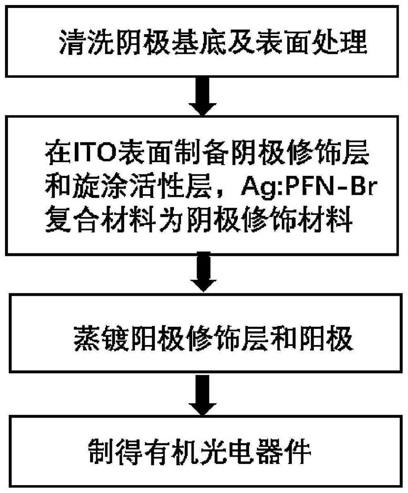
[0038] In this example, the Ag / PFN-Br composite interface is applied to the preparation of organic optoelectronic devices, and the organic optoelectronic devices are organic solar cells. The specific preparation steps are as follows:

[0039] (1) First clean the ITO glass to ensure that its surface is free of any contaminants. Put the ITO glass into deionized water, add 15mL of detergent, and then ultrasonicate for 20 minutes, repeat 2-3 times, and then wash with deionized water 2-3 times; then ultrasonically clean the ITO glass with isopropanol twice, each time 20 minutes; finally, put the ITO glass in an oven at 70°C for 12 hours and use it for later use.

[0040] (2) Move the treated ITO glass into the evaporation system, at 4 × 10 -4 Ag was evaporated to 1 nm under the pressure of Pa and placed in a nitrogen glove box. The pre-prepared PFN-Br solution (the weighed PFN-Br powder was added to methanol to dissolve, heated and stirred at 55 °C for 4 hours, the solution conc...

Embodiment 2

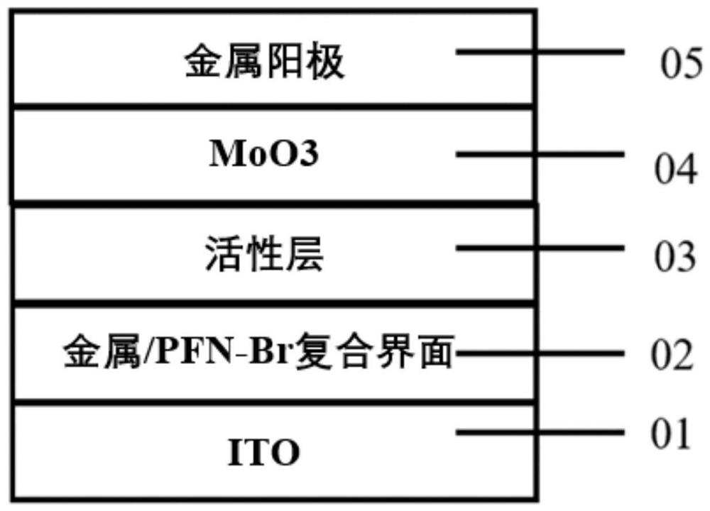
[0055] In this example, the Ag / PFN-Br composite interface is still applied to the preparation of flip-chip organic optoelectronic devices, the organic optoelectronic devices are organic solar cells, and the device structure is ITO / Ag / PFN-Br / PTB7-Th:PCBM / MoO 3 / Ag. The specific preparation steps are as follows:

[0056] (1) First clean the ITO glass to ensure that its surface is free of any contaminants. Put the ITO glass into deionized water, add 15mL of detergent, and then ultrasonicate for 20 minutes, repeat 2-3 times, and then wash with deionized water 2-3 times; then ultrasonically clean the ITO glass with isopropanol twice, each time 20 minutes; finally, put the ITO glass in an oven at 70°C for 12 hours and use it for later use.

[0057] (2) Move the treated ITO glass into the evaporation system, at 4 × 10 -4 Ag was evaporated to 1 nm under the pressure of Pa and placed in a nitrogen glove box. The pre-prepared PFN-Br solution (the weighed PFN-Br powder was added to...

Embodiment 3

[0066] This example applies the Ag / PFN-Br composite interface to the preparation of high-performance organic photodetectors. The preparation process is basically the same as the preparation method of the previous organic optoelectronic device (organic solar cell). The device structure is ITO / Ag / PFN-Br / PTB7-Th:COTIC-4F / MoO 3 / Al.

[0067] (1) First clean the ITO glass to ensure that its surface is free of any contaminants. Put the ITO glass into deionized water, add 15mL of detergent, and then ultrasonicate for 20 minutes, repeat 2-3 times, and then wash with deionized water 2-3 times; then ultrasonically clean the ITO glass with isopropanol twice, each time 20 minutes; finally, put the ITO glass in an oven at 70°C for 12 hours and use it for later use.

[0068] (2) Move the treated ITO glass into the evaporation system, at 4 × 10 -4 Ag was evaporated to 1 nm under the pressure of Pa and placed in a nitrogen glove box. The pre-prepared PFN-Br solution (the weighed PFN-Br p...


PUM

PropertyMeasurementUnit
thicknessaaaaaaaaaa
thicknessaaaaaaaaaa
thicknessaaaaaaaaaa

Abstract

The invention discloses an organic photoelectric device based on a metal-induced organic interface layer and a preparation method. According to the metal induced organic interface layer, a metal thin layer is pre-evaporated on the surface of a conductive electrode to serve as an induction layer, an organic material (such as PFN-Br) containing amino groups or other polar groups is spin-coated at room temperature, an induced dipole is generated through interaction between metal and the organic material, and a multifunctional composite interface is prepared. The method is applied to preparation of organic photoelectric devices such as organic solar cells and organic photoelectric detectors by a solution method. As a typical example, Ag / PFN-Br is adopted as a cathode interface modification layer to be applied to the organic photoelectric device, and strong chemical adsorption arrangement is formed on the surface of an electrode by the PFN-Br through the induction effect of Ag, so that a strong interface dipole is formed to regulate and control the surface potential of the electrode, the charge transfer barrier between an active layer and the electrode is reduced, and the performance of the organic photoelectric device is improved. And finally, high-efficiency and stable preparation of the organic photoelectric device is realized.

Description

technical field [0001] The invention belongs to the technical field of organic optoelectronic devices, and mainly relates to an organic optoelectronic device based on a metal-induced organic interface layer and a preparation method thereof. Background technique [0002] Organic optoelectronic devices have been widely studied due to their wide material sources, solution processability, and good mechanical properties, and have good application potential. With the synthesis and application of new materials with excellent performance and the continuous improvement of device preparation methods, the device performance of organic optoelectronic devices has been continuously improved. So far, the photoelectric conversion efficiency of organic optoelectronic devices has been greatly improved, which has greatly promoted the commercialization of organic optoelectronic devices. [0003] As a device composed of multiple layers of materials, the interface contact performance between dif...

Claims


Application Information

Patent Timeline
Patent Type & Authority Applications(China)
IPC IPC(8): H01L51/46H01L51/48H01L51/44
CPCH10K71/12H10K85/10H10K30/00H10K30/82Y02E10/549
Inventor 何志才冯闯宋云龙许聪娣
Owner SOUTH CHINA UNIV OF TECH
Why Eureka
Try Eureka