
Parameter extraction modeling method suitable for discrete device after scribing

A modeling method and discrete device technology, applied in instruments, special data processing applications, calculations, etc., can solve problems such as immature large signal models, failure analysis of new materials, and unclear defect structures, so as to improve the efficiency of circuit design, The effect of avoiding unevenness between sheets and saving research and development costs

Pending Publication Date: 2022-07-26
INST OF MICROELECTRONICS CHINESE ACAD OF SCI +1
View PDF0 Cites 0 Cited by
  • Summary
  • Abstract
  • Description
  • Claims
  • Application Information

AI Technical Summary

Problems solved by technology

[0004] In addition to the traditional silicon-based LDMOS and GaAs-based pHEMT, currently used RF power devices, gallium nitride (GaN) devices with higher power density are more and more widely used, but the large-signal model of these new material devices It is not yet mature, and the failure analysis of new materials, the defect structure is not clear, and there is still room for improvement in the process, which leads to the accuracy of the model not meeting the design requirements, especially for uniformity between sheets and dimensional diversity. The reason is that we need to adjust the die size in real time when we select the die size in the circuit design, and the commercial die has no connection form that can be tested on the chip, and only one-to-one testing can be performed through external circuits and bonding wires.

Method used


Image

  • Parameter extraction modeling method suitable for discrete device after scribing
  • Parameter extraction modeling method suitable for discrete device after scribing
  • Parameter extraction modeling method suitable for discrete device after scribing

Examples


Embodiment Construction

[0052] The preferred embodiments of the present invention are described below in detail with reference to the accompanying drawings, wherein the accompanying drawings constitute a part of the present application, and together with the embodiments of the present invention, serve to explain the principles of the present invention.

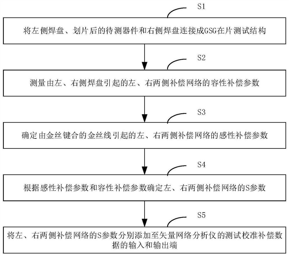
[0053] This embodiment discloses a parameter extraction modeling method suitable for discrete devices after dicing, such as figure 1 shown, including the following steps:

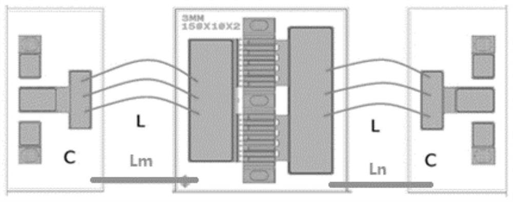
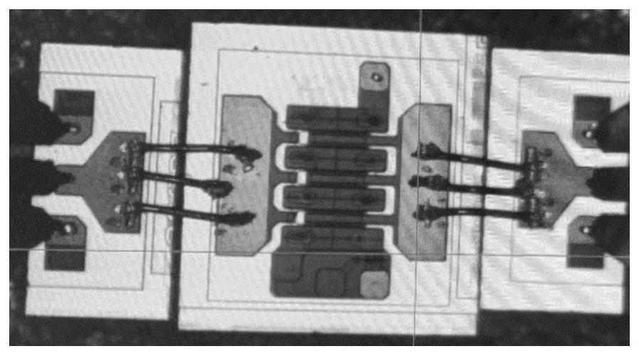
[0054]Step S1, connecting the left pad, the device under test after dicing, and the right pad by gold wire bonding to form a GSG on-chip test structure;

[0055] The device under test after dicing is a discrete device;

[0056] Specifically, the assembly sequence of the GSG (ground-signal-ground) on-chip test structure includes:

[0057] Solder the left and right pads and the device under test that connect the GSG on-chip test on the metal heat sink through solder;

[0058] Acc...


PUM


Abstract

The invention relates to a parameter extraction modeling method suitable for a discrete device after scribing. The method comprises the steps that a left side bonding pad, a to-be-tested device after scribing and a right side bonding pad are connected into a GSG on-chip testing structure in a gold wire bonding mode; capacitive compensation parameters of the left side compensation network and the right side compensation network caused by the left side bonding pad and the right side bonding pad are obtained through measurement; respectively determining inductive compensation parameters of left and right side compensation networks caused by gold wires bonded by gold wires based on the straight-through distances between the left and right side bonding pads and the to-be-tested device; determining S parameters of the left and right side compensation networks according to the inductive compensation parameters and the capacitive compensation parameters of the left and right side compensation networks; and respectively adding the S parameters of the compensation networks on the left side and the right side to the input end and the output end of test calibration compensation data of the vector network analyzer so as to remove the wiring influence of the GSG on-chip test structure. According to the method, the accurate large signal model can be quickly and effectively obtained, and model change caused by inter-chip non-uniformity of a device process is avoided.

Description

technical field [0001] The invention relates to the technical field of on-chip testing, in particular to a parameter-raising modeling method suitable for discrete devices after dicing. Background technique [0002] With the development and application of radio frequency devices, especially wide bandgap compound semiconductor devices, the operating frequency of the circuit is increased, and the output power is larger, especially the requirement for efficiency is accurate to 1%, so the power amplifier circuit, especially the mixed power The design of the amplifying circuit has higher and higher requirements on the model. [0003] Device models are the basis of circuit design. Power amplifier circuit design relies on accurate device models, especially nonlinear large-signal models. An accurate device model can significantly shorten the circuit design cycle, improve the design success rate, and reduce costs. [0004] In addition to the traditional silicon-based LDMOS and GaAs-b...

Claims


Application Information

Patent Timeline
Patent Type & Authority Applications(China)
IPC IPC(8): G06F30/373
CPCG06F30/373
Inventor 陈晓娟刘新宇丁武昌张昇李艳奎刘果果袁婷婷郑英奎魏珂金智
Owner INST OF MICROELECTRONICS CHINESE ACAD OF SCI
Learn More