
Semiconductor process chamber

A process chamber and semiconductor technology, which is applied in semiconductor/solid-state device manufacturing, discharge tubes, electrical components, etc., can solve the problems of reducing the stability of the machine, increasing the heat dissipation burden of the machine, and low efficiency of radio frequency power utilization. Heat generation, improved stability and reliability, and reduced ohmic loss

Pending Publication Date: 2022-07-26
BEIJING NAURA MICROELECTRONICS EQUIP CO LTD
View PDF0 Cites 0 Cited by
  • Summary
  • Abstract
  • Description
  • Claims
  • Application Information

AI Technical Summary

Problems solved by technology

[0004] However, in the existing inductively coupled plasma device, the RF power fed into the chamber by the upper RF power supply through the upper electrode is often partially lost in the form of ohmic heat, resulting in low utilization efficiency of the RF power and increasing the equipment cost. The heat dissipation burden reduces the stability of the machine work

Method used


Image

  • Semiconductor process chamber
  • Semiconductor process chamber
  • Semiconductor process chamber

Examples


Embodiment Construction

[0029] The specific embodiments of the present invention will be described in detail below with reference to the accompanying drawings. It should be understood that the specific embodiments described herein are only used to illustrate and explain the present invention, but not to limit the present invention.

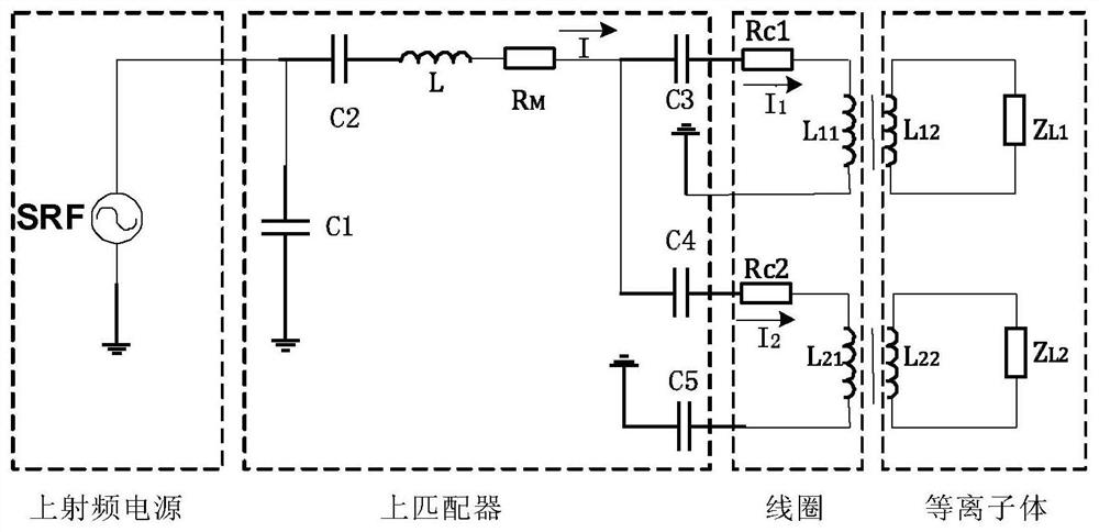
[0030] The equivalent circuit of the RF circuit of the upper electrode in the existing inductively coupled plasma device is as follows: figure 1 As shown, the upper RF power source (Source Generator) loads power to the coil (Coil) of the upper electrode through the upper matcher (Source Match), and the RF energy on the coil is coupled into the chamber through the dielectric window, thereby exciting the chamber. The process gas generates plasma, which acts on the wafer and can be used in processes such as wafer etching and deposition.

[0031] For the upper electrode RF circuit, the power of the upper RF power supply is mainly consumed by the loss power of the matcher, t...


PUM


Abstract

The invention provides a semiconductor process chamber which comprises a cavity, a chuck arranged in the cavity and an upper electrode assembly arranged above the cavity, the upper electrode assembly comprises an upper radio frequency power supply, an upper matcher and at least one radio frequency coil, and the upper radio frequency power supply is used for providing radio frequency power for the radio frequency coil through the upper matcher; the upper electrode assembly further comprises at least one shunt capacitor, the first end of the radio frequency coil is connected with the upper matcher, the second end of the radio frequency coil is grounded, and the shunt capacitor is connected between the first end and the second end of the corresponding radio frequency coil. The shunt capacitor and the corresponding radio frequency coil have a natural resonant frequency not lower than the working frequency of the radio frequency power supply. In the invention, the shunt capacitor and the corresponding radio frequency coil have the natural resonant frequency not lower than the working frequency, so that the ohmic loss on the radio frequency coil can be effectively reduced, the radio frequency feed-in efficiency of the upper electrode is improved, and the stability and reliability of a machine table are further improved.

Description

technical field [0001] The present invention relates to the field of semiconductor process equipment, in particular, to a semiconductor process chamber. Background technique [0002] Deep silicon etching has important applications in the fields of integrated circuits (Integrated circuit, IC), Micro-Electro-Mechanical System (MEMS) and advanced packaging, and is a very important process in industrial production. Since traditional wet etching belongs to isotropic etching, only anisotropic dry etching can achieve deep silicon etching. Low-temperature plasma technology is an important foundation in dry etching. Among them, Inductively Coupled Plasma (ICP) and Capacitively Coupled Plasma (CCP) are commonly used in dry etching and thin film deposition in the semiconductor field. plasma source. Among them, the inductively coupled plasma source excites the gas to generate plasma by the high-frequency electromagnetic field generated by the high-frequency current passing through the...

Claims


Application Information

Patent Timeline
Patent Type & Authority Applications(China)
IPC IPC(8): H01J37/32H01L21/67
CPCH01J37/32568H01J37/32183H01J37/3211H01L21/67069H01L21/67213H01J2237/3345
Inventor 王松陈星赵晋荣韦刚
Owner BEIJING NAURA MICROELECTRONICS EQUIP CO LTD
Learn More