Supercharge Your Innovation With Domain-Expert AI Agents!

Thin film transistor and manufacturing method thereof

A technology of thin film transistors and manufacturing methods, applied in the direction of transistors, semiconductor/solid-state device manufacturing, semiconductor devices, etc., can solve the problems of high sub-threshold swing, weakened gate control ability, and reduced turn-on current, so as to reduce sub-threshold swing , Improve the effect of opening current

Pending Publication Date: 2022-07-29
SHENZHEN ROYOLE TECH CO LTD
View PDF0 Cites 0 Cited by
  • Summary
  • Abstract
  • Description
  • Claims
  • Application Information

AI Technical Summary

Problems solved by technology

Wherein, after the active layer is completed, when the drain / source electrode 15 is etched, the etchant will cause damage to the active layer 14, such as figure 2 As shown, the surface of the active layer 14 produces more defects
First, when figure 1 When the bottom-gate thin film transistor shown is turned on, the defects will trap carriers, resulting in reduced turn-on current and weakened gate control capability
Second, the defect will lead to higher subthreshold swing and lower stability when the bottom gate TFT is turned on

Method used


Image

  • Thin film transistor and manufacturing method thereof
  • Thin film transistor and manufacturing method thereof
  • Thin film transistor and manufacturing method thereof

Examples


Embodiment Construction

[0058] The present invention will be described in detail below with reference to specific embodiments. The following examples will help those skilled in the art to further understand the present invention, but do not limit the present invention in any form. It should be noted that, for those skilled in the art, several modifications and improvements can be made without departing from the concept of the present invention. These all belong to the protection scope of the present invention.

[0059] In order to make the purpose, technical solutions and advantages of the present application more clearly understood, the present application will be described in further detail below with reference to the accompanying drawings and embodiments. It should be understood that the specific embodiments described herein are only used to explain the present application, but not to limit the present application.

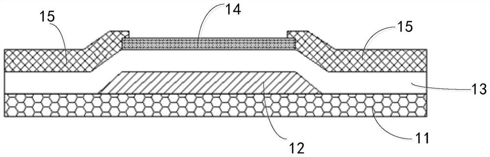
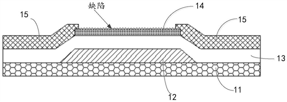
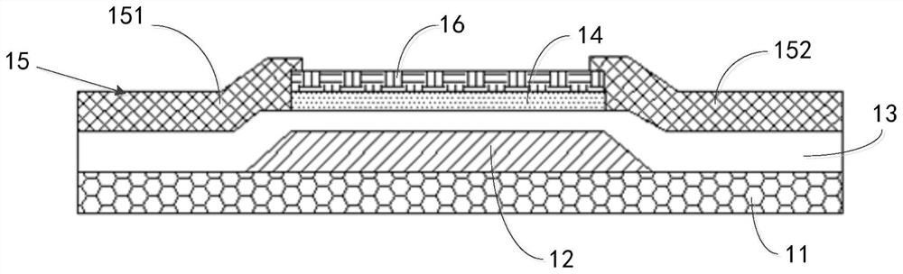
[0060] It should be noted that, if there is no conflict, various features in th...


PUM


Abstract

The embodiment of the invention relates to the technical field of display panels, in particular to a thin film transistor and a manufacturing method thereof, for the thin film transistor, a first active layer can be protected by a second active layer, and structural defects cannot be caused to the first active layer when a drain-source layer is etched. Therefore, when a positive voltage is applied to the first gate electrode, carriers deviate towards the surface, close to the first gate dielectric layer, of the first active layer and are not captured, a stable carrier transport channel (a first conductive channel) can be formed, the turn-on current can be improved, and the sub-threshold swing can be reduced. Besides, based on the fact that the Fermi level of the second active layer is higher than that of the first active layer, when the thin film transistor is communicated for electric conduction, electrons drift from the second active layer with the high Fermi level to the first active layer with the low Fermi level, more electrons participate in electric conduction in the first conducting channel, and the conductivity of the thin film transistor is improved. And the turn-on current of the thin film transistor can be further effectively improved.

Description

technical field [0001] Embodiments of the present invention relate to the technical field of display panels, and in particular, to a thin film transistor and a method for manufacturing the same. Background technique [0002] Thin film transistors (TFTs) are an important part of display panels. TFTs can be formed on glass substrates or plastic substrates and used as switching and driving components in flat display devices such as LCD and OLED. The thin film transistor includes a single-gate thin-film transistor (Single-Gate TFT) and a double-gate thin-film transistor (Double-Gate TFT). Wherein, the single-gate thin film transistor includes a top-gate thin-film transistor and a bottom-gate thin-film transistor, wherein the gate and insulating layer of the bottom-gate thin-film transistor can simultaneously serve as an optical protective layer, thereby avoiding the generation of photo-generated carriers and having Good electrical stability, can be widely used. In addition, th...

Claims


Application Information

Patent Timeline
IPC IPC(8): H01L29/10H01L29/786H01L21/336
CPCH01L29/1033H01L29/78693H01L29/66969
Inventor 黄德猛
Owner SHENZHEN ROYOLE TECH CO LTD
Features
  • R&D
  • Intellectual Property
  • Life Sciences
  • Materials
  • Tech Scout
  • Unparalleled Data Quality
  • Higher Quality Content
  • 60% Fewer Hallucinations
Learn More