Band-gap reference circuit with second-order curvature compensation
A reference circuit and curvature compensation technology, applied in the circuit field, can solve the problems of not meeting the high performance requirements of the chip, and achieve the effect of saving area and low temperature drift
- Summary
- Abstract
- Description
- Claims
- Application Information
AI Technical Summary
Problems solved by technology
Method used
Image
Examples
Embodiment 2
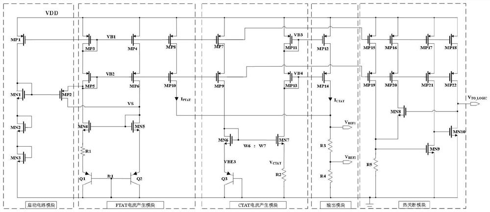
[0068] The CTAT current generation module, output module and thermal shutdown module of the present invention are similar to those in Embodiment 1. The current mirrors in the three modules in Embodiment 1 all adopt a cascode structure, and those in Embodiment 2 all adopt a common current mirror structure.
[0069] refer to Figure 4 , PTAT current generation module includes 2 PMOS tubes MP3, MP4, 2 PNP transistors Q1 and Q2, 1 resistor R1 and an operational amplifier AMP. The sources of the PMOS transistors MP3 and MP4 are connected to the power supply voltage VDD, the gates are connected, the drain of the PMOS transistor MP3 is connected to one end of the resistor R1 and the positive input end of the operational amplifier, and the drain of the PMOS transistor MP4 is connected to the emitter of Q2 and the operational amplifier. The negative input terminal of the operational amplifier; the output of the operational amplifier is connected to the gates of the PMOS transistor MP3 ...
PUM
 Abstract
Description
Claims
Application Information


