DC offset cancellation circuit and method

A technology to eliminate circuits and circuits, applied in the direction of improving amplifiers to reduce nonlinear distortion, improving amplifiers to reduce temperature/power supply voltage changes, differential amplifiers, etc., can solve the problems of large quiescent current and low power consumption, etc., to achieve Strong driving capability, correction of common-mode voltage, and correction of differential-mode offset effects

Pending Publication Date: 2022-08-05
XI AN JIAOTONG UNIV
View PDF0 Cites 0 Cited by
  • Summary
  • Abstract
  • Description
  • Claims
  • Application Information

AI Technical Summary

Problems solved by technology

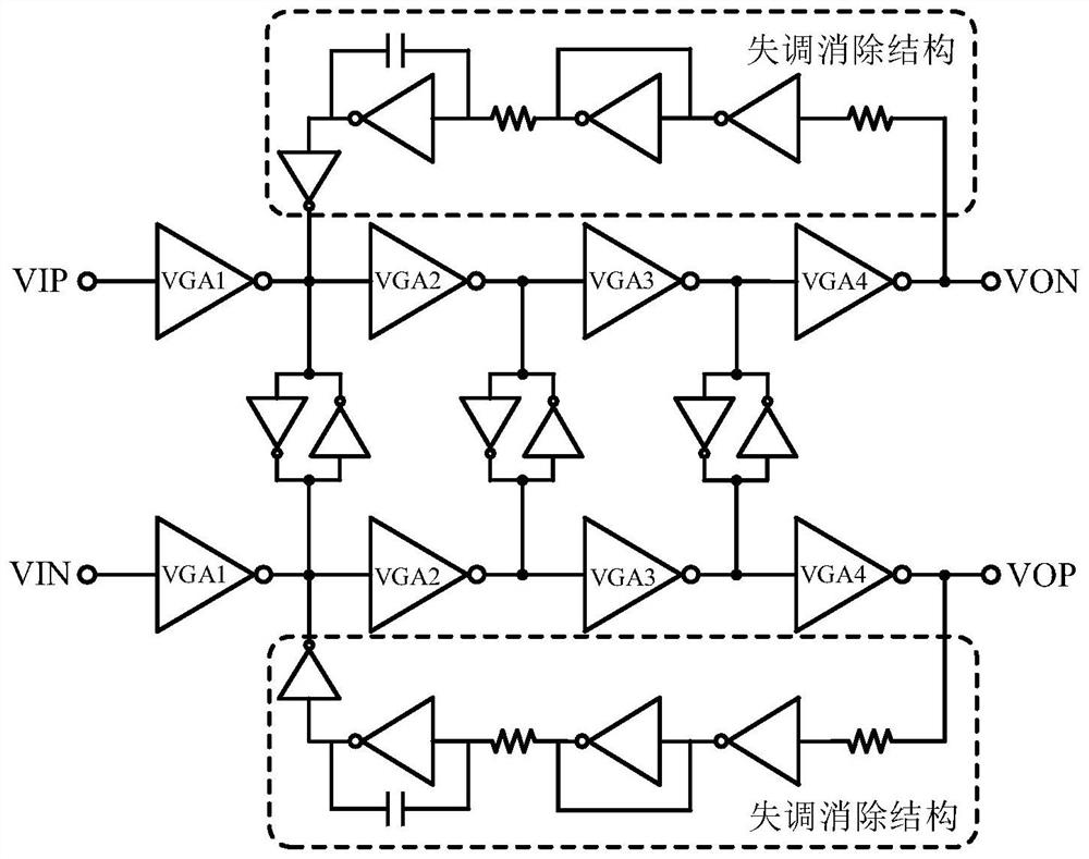
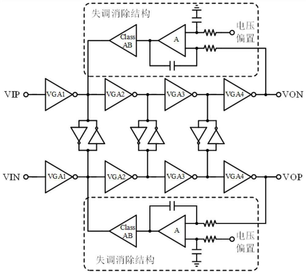
[0004] The purpose of the present invention is to provide a DC offset elimination circuit and method, which not only realizes the calibration of the differential mode offset, but also realizes the correction of the common mode voltage, and also solves the problem that the existing offset elimination structure does not consider low power consumption. Therefore, the problem of large quiescent current

Method used


Image

  • DC offset cancellation circuit and method
  • DC offset cancellation circuit and method
  • DC offset cancellation circuit and method

Examples


Embodiment Construction

[0033] The technical solutions in the embodiments of the present invention will be clearly and completely described below with reference to the accompanying drawings in the embodiments of the present invention. Obviously, the described embodiments are part of the embodiments of the present invention, but not all of the embodiments. Based on the embodiments of the present invention, all other embodiments obtained by those of ordinary skill in the art without creative efforts shall fall within the protection scope of the present invention.

[0034] In the description of the present invention, it should be noted that the terms "installed", "connected" and "connected" should be understood in a broad sense, unless otherwise expressly specified and limited, for example, it may be a fixed connection or a detachable connection Connection, or integral connection; can be mechanical connection, can also be electrical connection; can be directly connected, can also be indirectly connected ...


PUM


Abstract

The invention discloses a DC offset cancellation circuit and method. The DC offset cancellation circuit comprises an offset cancellation module, an amplifier group and a phase inverter structure, the inverter structures are connected between the two amplifier groups, one end of each amplifier group is connected with a signal input end, and the other end of each amplifier group is connected with a signal output end; an offset elimination module is arranged between the input end and the output end of each amplifier group; the structure of the circuit is different from an existing offset elimination circuit structure, common-mode voltage can be corrected, differential-mode offset can be corrected, and the working reliability of the circuit is improved. An output DC point is stabilized at an optimal bias point in a single-end bias mode, and for an amplifier with an inverter structure, it can be ensured that the amplifier works in a state with the best linearity, and then the requirement for the linearity of a whole circuit is met. Static power consumption can be greatly reduced by the Class AB output stage, waste of current on a transconductance tube is avoided, and the driving capability is much stronger than that of a single transconductance tube.

Description

technical field [0001] The invention belongs to the technical field of optical communication chip design, and in particular relates to a DC offset elimination circuit and method. Background technique [0002] With the increase of data transmission rate year by year, optical carrier plays an important role in the field of communication with its huge capacity. In the optical communication system, the optical receiver is used to convert the current signal into a voltage signal, amplify the current into a voltage signal through a transimpedance amplifier, and then amplify the output through the post-stage. missing role. Especially for the amplifier circuit with inverter structure, if the circuit has a relatively large differential mode offset, due to the large gain from the pre-stage to the output, the output may be saturated eventually, thus affecting the performance of the circuit. [0003] In order to solve this problem, the existing method adopts two single-ended inverter ...

Claims


Application Information

Patent Timeline
Patent Type & Authority Applications(China)
IPC IPC(8): H03F1/30H03F1/32H03F1/02H03F3/45H03F3/68
CPCH03F1/30H03F1/32H03F1/0205H03F3/45479H03F3/68H03F2203/45028
Inventor 李丹师文博夏翼飞
Owner XI AN JIAOTONG UNIV
Why Eureka
Try Eureka