
Electronic component

A technology of electronic components and circuits, applied in the directions of printed circuit components, electrical components, circuits, etc., can solve problems such as difficulty in designing electronic components

Inactive Publication Date: 2004-08-11
PANASONIC CORP
View PDF0 Cites 0 Cited by
  • Summary
  • Abstract
  • Description
  • Claims
  • Application Information

AI Technical Summary

Problems solved by technology

Therefore, expertise is required to prevent electromagnetic shielding from being weakened, which makes it difficult to design electronic components

Method used


Image

  • Electronic component
  • Electronic component
  • Electronic component

Examples


Embodiment Construction

[0012] Embodiments of the present invention are described below with reference to the accompanying drawings.

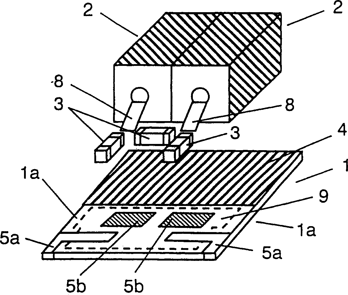
[0013] figure 1 is a partially exploded perspective view of a dielectric filter. The dielectric filter includes circuit elements such as dielectric resonators 2, chip capacitors 3 and others mounted on a substrate 1 by reflection flow soldering.

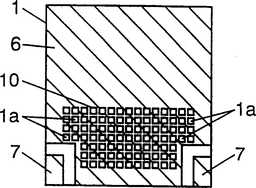
[0014] The substrate 1 comprises a rectangular bare substrate 1a made of glass epoxy resin. On the upper surface of the substrate 1, the following parts are provided: a) a ground electrode 4 for mounting the dielectric resonator 2, b) partially formed circuit electrodes 5a and 5b for mounting and connecting the chip capacitor 3 and others element. On the lower surface, a ground electrode 6 is provided to cover substantially the entire surface, as figure 2 As shown in , and the input / output electrodes 7 are provided at both ends of one side. Circuit electrodes 5a on the upper surface are coupled to input / output electrod...


PUM


Abstract

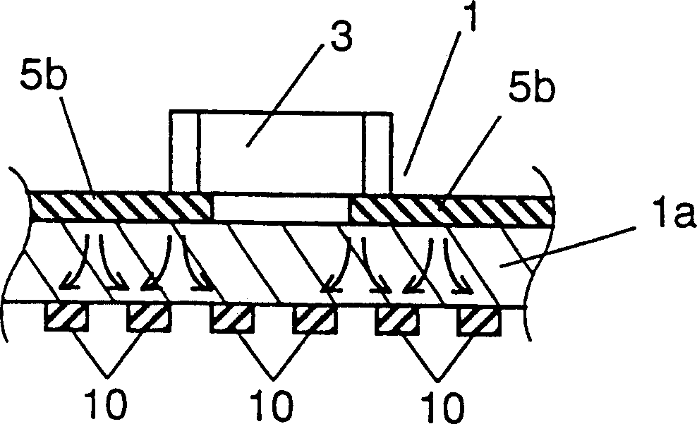
The invention provides a surface-mount electronic component arranged on, e.g., a printing wiring assembly board through heat treatment, such as reflow welding and the like. An exposed substrate base is made exposed through mesh parts. An electrode is formed into a reticulated form so that each side of the independent mesh electrode parallels to each edge of the substrate base, while width of the mesh electrode block is less than that of the exposed substrate base. The structure can ensure high-level planarity of the mounting surface of the electronic component without impairing shielding efficiency thereof.

Description

technical field [0001] The present invention relates to surface mount electronic components which are soldered to, for example, printed wiring assembly boards (herein referred to as PWAs) by a heating step such as reflected flow soldering. Background technique [0002] Conventional electronic components used in surface mounting and soldered to PWAs by a heating step such as reflected flow soldering comprise a substrate having an upper surface and a lower surface. The upper surface is provided with a plurality of electrodes on which circuit elements are mounted. The lower surface of the element is provided with ground electrodes, which cover substantially the entire lower surface to enhance electromagnetic shielding. [0003] Since the lower surface of the electronic component described above is a mounting surface to be surface-mounted to the PWA, the lower surface requires precise flatness. In order to meet this need, a method is used in which at least one non-electrode po...

Claims


Application Information

Patent Timeline
IPC IPC(8): H05K1/18H01H47/00H01P1/205H05K1/02H05K3/30
Inventor 北雅己田中正治织田学
Owner PANASONIC CORP
Learn More