Semiconductor device manufacturing process

A manufacturing method and semiconductor technology, applied in semiconductor/solid-state device manufacturing, semiconductor devices, semiconductor/solid-state device components, etc., can solve the problems of limited miniaturization, improve reliability, simplify procedures, and prevent loosening Effect

Inactive Publication Date: 2004-08-18
SAMSUNG ELECTRONICS CO LTD
View PDF0 Cites 4 Cited by
  • Summary
  • Abstract
  • Description
  • Claims
  • Application Information

AI Technical Summary

Problems solved by technology

Most of them bond wires or wires to the electrodes of semiconductor chips for electric

Method used


Image

  • Semiconductor device manufacturing process
  • Semiconductor device manufacturing process
  • Semiconductor device manufacturing process

Examples


no. 1 Embodiment

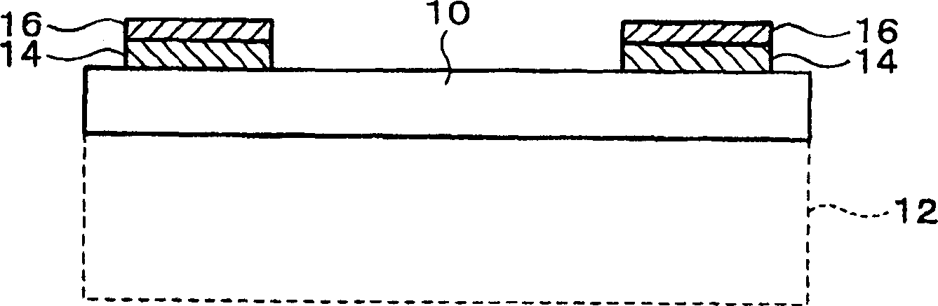
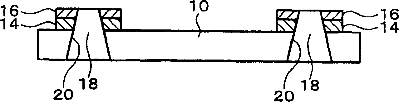
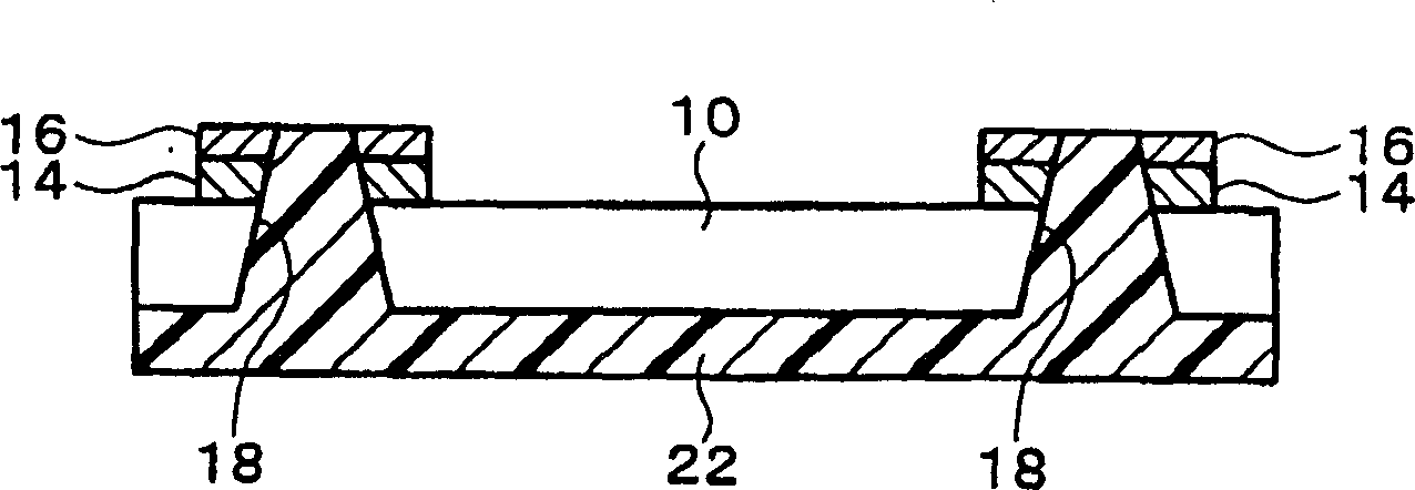
[0051] Figure 1A ~ 2C It is a schematic diagram of the manufacturing method of the semiconductor device according to the first embodiment of the present invention. Figure 1Ais a schematic diagram of a semiconductor chip 10 (semiconductor element) used in this embodiment. In the example shown in this embodiment, a semiconductor wafer diced into a plurality of semiconductor chips 10 side by side is used. The semiconductor chip 10 is generally a rectangular parallelepiped (including a cube), but its shape is not limited and may be spherical.

[0052] The semiconductor chip 10 is formed by thinning the thickness of the original semiconductor chip 12 (or semiconductor wafer). Specifically, the surface of the semiconductor chip 10 opposite to the surface on which the integrated circuit is formed (active surface) is polished. The thickness of the semiconductor chip 10 can be reduced as much as possible as long as the portion forming the integrated circuit remains. The thickness...

no. 2 Embodiment

[0092] Figure 4A and Figure 4B It is a schematic diagram of a method of manufacturing a semiconductor device according to a second embodiment of the present invention. In this embodiment, the method of forming the conductive member 28 is different from the above.

[0093] like Figure 4A As shown, in this embodiment, first and second semiconductor chips 11 and 13 are provided. The first and second semiconductor chips 11 and 13 can form the second through-holes 24 penetrating through at the positions of the electrodes 14 of the respective semiconductor chips through the above steps. In this embodiment, the conductive member is solid and disposed inside the second through hole 24 of the second semiconductor chip 13 . The conductive member may also be a bump 32 . The bumps 32 can be formed of solder, gold, or the like.

[0094] The bumps 32 are provided and connected to the electrodes 14 (plating layer 16 ) of the first semiconductor chip 11 . Specifically, when the firs...

no. 3 Embodiment

[0108] Figure 6A and 6B It is a schematic diagram of the manufacturing method of the semiconductor device according to the third embodiment of the present invention. In this embodiment, the form of the second through hole 25 is different from the above.

[0109] like Figure 6A As shown, in this embodiment, the second through hole 25 is formed with a conical surface. Specifically, the second through hole 25 may be formed with a conical surface 27 that becomes smaller as it is farther away from the electrode 14 of the semiconductor chip 10 . The second through hole 25 can be formed, for example, by irradiating a laser beam from the electrode 14 side of the semiconductor chip 10 , or by irradiating a laser beam from the side opposite to the electrode 14 . In addition, other forms and formation methods of the second through hole 25 are as described above.

[0110] Figure 6B The semiconductor chip 10 having the above-mentioned second through hole 25 is a schematic diagram ...


PUM


Abstract

To provide a semiconductor device and method of manufacturing the same, circuit board, and electronic apparatus, where electrical connections can be established easily with high reliability. The method of manufacturing the semiconductor device includes a first process of forming first through-holes 18 at, places where electrodes 14 are formed, in a semiconductor element 10 provided with the electrodes; a second process of providing an insulating material 22 in a region, including the inside parts of the first through-holes 18, so that second through holes 24 which pass through the insulating material 22 are formed; and a third process of providing a conductive member 28 inside the first through-holes 18 so that it passes through the second through-holes 24.

Description

technical field [0001] The present invention relates to a method of manufacturing a semiconductor device. Background technique [0002] In recent years, semiconductor devices having a laminated structure in which a plurality of semiconductor chips are stacked are being developed. Most of them bond wires or wires to electrodes of the semiconductor chip for electrical connection, but there is a limit to miniaturization in order to install wires and the like. Contents of the invention [0003] The present invention was conceived to solve this problem, and an object of the present invention is to provide a method for manufacturing a semiconductor device that can easily realize electrical connection with high reliability. [0004] According to the present invention, there is provided a method of manufacturing a semiconductor device, comprising: on a semiconductor element having electrodes, a first step of forming a through-hole first through hole at the position of the electro...

Claims


Application Information

Patent Timeline
IPC IPC(8): H01L23/12H01L21/768H01L21/98H01L23/48H01L23/485H01L25/065H01L25/07H01L25/18
CPCH01L2224/83851H01L2224/13009H01L24/83H01L25/0657H01L2224/16145H01L2924/0105H01L2924/01082H01L2225/06586H01L2224/13025H01L2924/01004H01L2224/81801H01L2224/0557H01L2225/06541H01L2224/13144H01L2924/01029H01L2924/00013H01L2924/19041H01L2924/014H01L2924/01013H01L24/90H01L25/50H01L24/81H01L2924/19043H01L2224/1134H01L2924/01079H01L2224/1308H01L2224/81136H01L2924/14H01L2225/06513H01L2924/01005H01L2924/01033H01L2924/01006H01L21/76898H01L2924/01078H01L2224/90H01L2224/131H01L23/481H01L2924/01075H01L24/10H01L24/03H01L24/05H01L24/11H01L24/13H01L2224/023H01L2224/0401H01L2224/05124H01L2224/05147H01L2224/05576H01L2224/05644H01L2224/05655H01L2224/0579H01L2224/058H01L2224/11H01L2224/13H01L2224/1329H01L2224/133H01L2224/16146H01L2224/16235H01L2924/00011H01L2924/0002H01L2924/12042H01L2924/351H01L2224/13099H01L2924/3512H01L2924/00H01L2224/05552H01L2924/00014H01L2924/0001
Inventor 仓岛羊平梅津一成伊东春树
Owner SAMSUNG ELECTRONICS CO LTD
Why Eureka
Try Eureka