Check patentability & draft patents in minutes with Patsnap Eureka AI!

Nano multicrystal biofilm photoelectric cell and its manufacturing method

A biofilm and production method technology, applied in the fields of nanostructure manufacturing, nanotechnology, photovoltaic power generation, etc., can solve the problems of high production and application costs, and the inability to popularize and apply in large quantities.

Inactive Publication Date: 2004-11-10
徐瑞松
View PDF0 Cites 0 Cited by
  • Summary
  • Abstract
  • Description
  • Claims
  • Application Information

AI Technical Summary

Problems solved by technology

[0002] Solar cells have developed rapidly in recent years and have been applied in certain fields, but their high production and application costs prevent them from being widely used

Method used


Image

  • Nano multicrystal biofilm photoelectric cell and its manufacturing method
  • Nano multicrystal biofilm photoelectric cell and its manufacturing method
  • Nano multicrystal biofilm photoelectric cell and its manufacturing method

Examples


Embodiment Construction

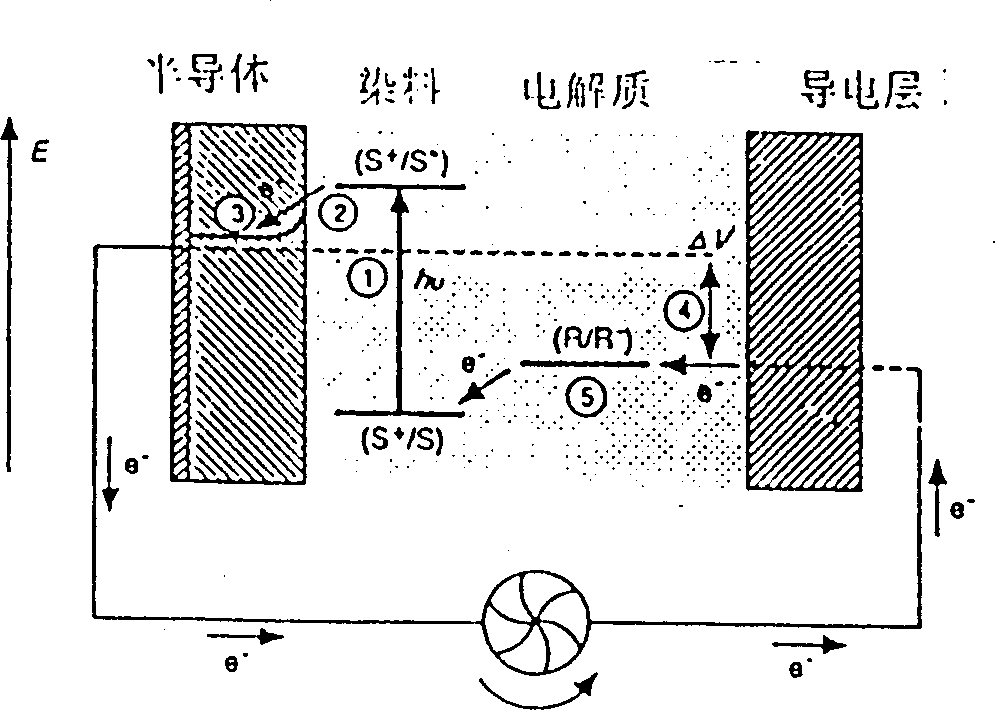
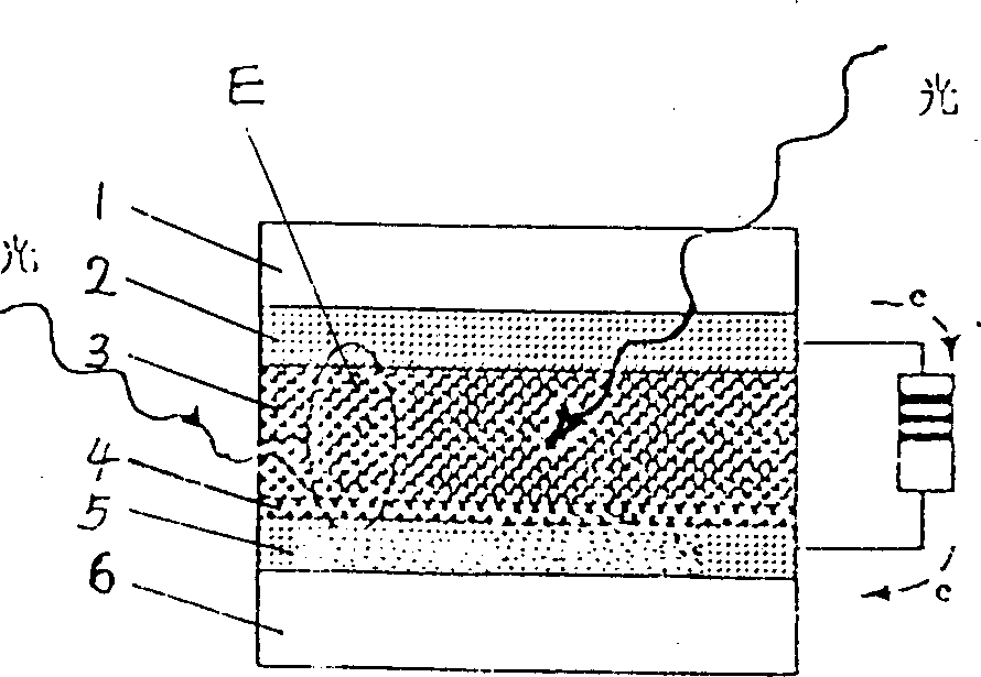
[0030] Such as figure 2 , image 3 The structure of the nano-polycrystalline biological thin film photovoltaic cell shown is as follows: it consists of a layered structure, and the structure from top to bottom is:

[0031] 1. Light-transmitting plastic film cover layer, its light transmittance is greater than 85%, and it can withstand high temperature of 200°C;

[0032] 2. SnO made by magnetron sputtering 2 Conductive film layer, film thickness 20μm, resistance less than 10Ω;

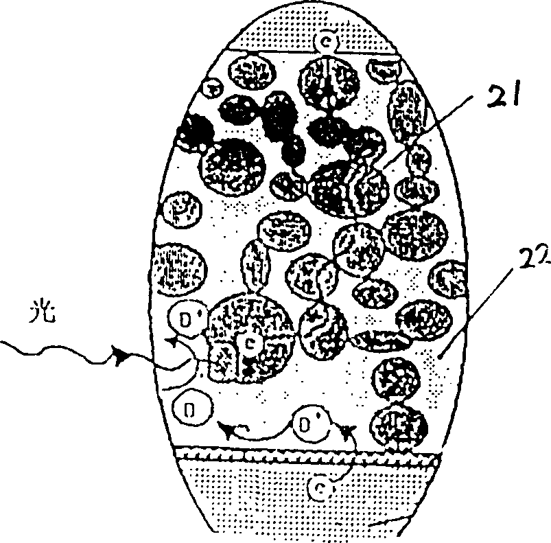
[0033] 3. Pd, Rh, Ru and other organic or inorganic dyes, ZnO, ZnS, Nb 2 o 2 or TiO 2 A semiconductor film with holes self-assembled from a semiconductor film and a latex-like redox agent, with a film thickness of 10-20 μm;

[0034] 4. The conductive film made of Ag, Au or Pt, etc., has excellent electron transfer performance, and the film thickness is 10 μm;

[0035] 5. SnO made by magnetron sputtering 2 Conductive film layer, film thickness 20μm, resistance less than 10Ω;

[0036] 6. Rollabl...


PUM


Abstract

A biological film photocell with nanometre polycrystal has the structure from bottom to top with 1) covering layer of light transmission plastic film, 2) SnO2 conductive film layer, 3) organic or inorganic photosensitive dyestuff ZnO, ZnS, Nb2O2 or TiO2 semiconductor film and semiconductor film with cavities self-assembled by redox in latex state, 4) Ag, Au, P+ conductive film, 5) SiO2 conductivefilm and 6) bed course for thin plate. The preparing steps for it is as follows, 1) spraying conductive solution on the bed course of conductive film and drying it by vacuum 2) coating InO, ZnS latexfilm by the screen printing method and drying it by vacuum, 3) putting the product produced by step 2) into organic or inorganic dyestuff for soaking and then drying it by wind blowing.

Description

Technical field: [0001] The invention relates to a solar cell and a manufacturing method thereof, in particular to a nanometer material biological film photocell and a manufacturing method thereof. Background technique: [0002] Solar cells have developed rapidly in recent years and have been applied in certain fields, but their high production and application costs prevent them from being widely used. Invention content: [0003] The object of the present invention is to provide a nano-polycrystalline bio-film photoelectric cell with low production and application costs, and provide its manufacturing method. [0004] In order to achieve the above object, the nano-polycrystalline biological thin film photovoltaic cell provided by the present invention has the following structure: it is made up of layered structure, and the structure from top to bottom is: [0005] ①Light-transmitting plastic film cover layer, [0006] ②SnO 2 conductive layer, [0007] ③ Organic or inorg...

Claims


Application Information

Patent Timeline
Patent Type & Authority Patents(China)
IPC IPC(8): B82B1/00B82B3/00H01G9/20H01L31/18H10K99/00
CPCH01G9/2059H01G9/2031B82Y10/00H01L51/0093Y02E10/542Y02P70/50H10K85/761
Inventor 徐瑞松
Owner 徐瑞松
Features
  • R&D
  • Intellectual Property
  • Life Sciences
  • Materials
  • Tech Scout
  • Unparalleled Data Quality
  • Higher Quality Content
  • 60% Fewer Hallucinations
Learn More