Electrochemical glass and silicon chip perforator

A glass sheet and electrochemical technology, applied in metal processing and other directions, can solve the problems of glass or silicon sheet damage, unfavorable batch processing, and rising costs, and achieve the effects of fast perforation speed, no destructive damage, and simple structure

Inactive Publication Date: 2005-03-09
HARBIN INST OF TECH
View PDF0 Cites 0 Cited by
  • Summary
  • Abstract
  • Description
  • Claims
  • Application Information

AI Technical Summary

Problems solved by technology

The main disadvantage of this method is that the time is too long, which is not conducive to batch processing
At the same time, it is easy to cause damage to the glass sheet or silicon sheet, which increases the cost

Method used


Image

  • Electrochemical glass and silicon chip perforator
  • Electrochemical glass and silicon chip perforator

Examples


Embodiment 1

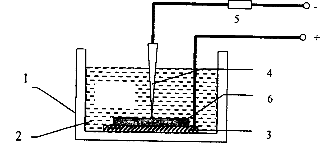
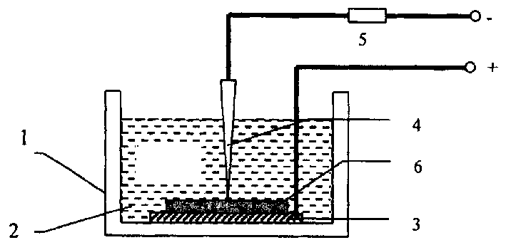
[0010] Embodiment 1, the composition of the device for perforating glass sheets and silicon sheets by the electrochemical method includes an electrolytic cell 1, in which a sodium bicarbonate solution 2 with a concentration of 20% is installed, and the negative electrode 3 of the electrolytic cell is a graphite electrode or a nickel electrode, The perforation probe 4 is used as the anode of the electrolytic cell. The material of the perforation probe is metal tungsten. The current-limiting resistor 5 is connected in series on the perforation probe. A pulsating DC voltage is applied between the perforation probe and the negative electrode. The voltage range is 40-100V.

Embodiment 2

[0011] Embodiment 2, the composition of the device for perforating glass sheets and silicon sheets by the electrochemical method includes an electrolytic cell 1, in which a potassium hydroxide solution 2 with a concentration of 40% is installed, and the negative electrode 3 of the electrolytic cell is a graphite electrode or a nickel electrode, The perforation probe 4 is used as the anode of the electrolytic cell. The material of the perforation probe is metal tungsten. The current-limiting resistor 5 is connected in series on the perforation probe. A pulsating DC voltage is applied between the perforation probe and the negative electrode. The voltage range is 40-100V.

[0012] During processing, according to the connection structure shown in the accompanying drawings, after the connection is completed, the probe is placed at the place where the glass sheet or the silicon sheet 6 needs to be perforated. Processing can be carried out by applying a pulsating DC voltage in the ran...


PUM


Abstract

The electrochemical glass and silicon chip perforator includes electrolyzer with alkali solution held, graphite electrode or nickel electrode connected to power source negative pole and perforating probe of tungsten metal connected to power source positive pole via a current limiting resistor. The glass and silicon chip is set horizontally on the graphite electrode or the nickel electrode, and the power soure provides pulsed DC voltage of 40-100 V. The present invention has the advantages of fast perforating speed, simple structure, easy operation and carrying about, and no damage to the surface of the glass and silicon chip.

Description

(1) Technical field [0001] The invention relates to a processing device, especially a device for making a through hole on a glass sheet or a silicon sheet, which is often used in the processing of MEMS micromechanical devices. (2) Background technology [0002] Making vias in glass or silicon wafers is a specialized technology in the microelectronics and MEMS fields. In the preparation process of various sensors, the problem of making electrode lead holes on glass or silicon wafers is often encountered. [0003] At present, the methods for perforating silicon wafers and glass wafers mainly include chemical etching and mechanical grinding. The chemical etching method must utilize a masked photolithography process. This method not only has a complicated process, but also destroys the flatness of the silicon wafer and glass wafer surface during the manufacturing process. If bonding and other processes that require extremely high surface flatness are involved in the subsequen...

Claims


Application Information

Patent Timeline
Patent Type & Authority Patents(China)
IPC IPC(8): B26F1/26B26F1/28
Inventor 刘晓为霍明学王喜莲蓝慕杰陈伟平
Owner HARBIN INST OF TECH
Why Eureka
Try Eureka