Trench MOSFET device with double-diffuser distribution and making method

A trench and device technology, applied in semiconductor/solid-state device manufacturing, semiconductor devices, electrical components, etc., can solve the problem of device breakdown voltage reduction, achieve low on-resistance, prevent breakdown, and avoid reduction

Inactive Publication Date: 2005-09-21
GEN SEMICON
View PDF3 Cites 0 Cited by
  • Summary
  • Abstract
  • Description
  • Claims
  • Application Information

AI Technical Summary

Problems solved by technology

However, when reducing the depth of the trench and the P-body junction depth, the device breakdown voltage decreases in the end region due to the shallower P-body junction in the end region
[0008] Consequently, efforts to provide low unit on-resistance for trench DMOS by increasing cell density have recently been hampered by concurrent detrimental changes, such as those related to device threshold voltage, gate charge, and / or end-region device breakdown voltage. The problem

Method used


Image

  • Trench MOSFET device with double-diffuser distribution and making method
  • Trench MOSFET device with double-diffuser distribution and making method
  • Trench MOSFET device with double-diffuser distribution and making method

Examples


Embodiment Construction

[0051] The invention is explained in more detail below with reference to the accompanying drawings, in which preferred embodiments of the invention are shown. The invention can, however, be embodied in different ways and should not be limited to the embodiments described herein. For example, the description here refers more to N-channel 20 to 30V devices, but clearly other devices are possible.

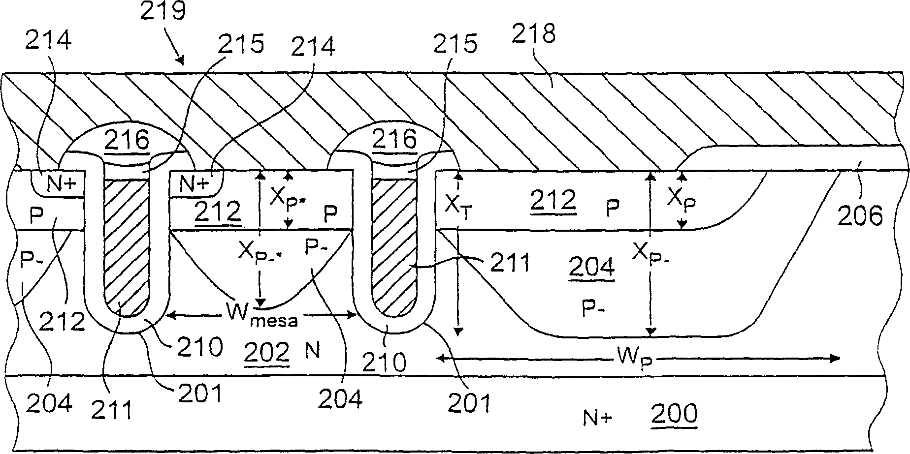
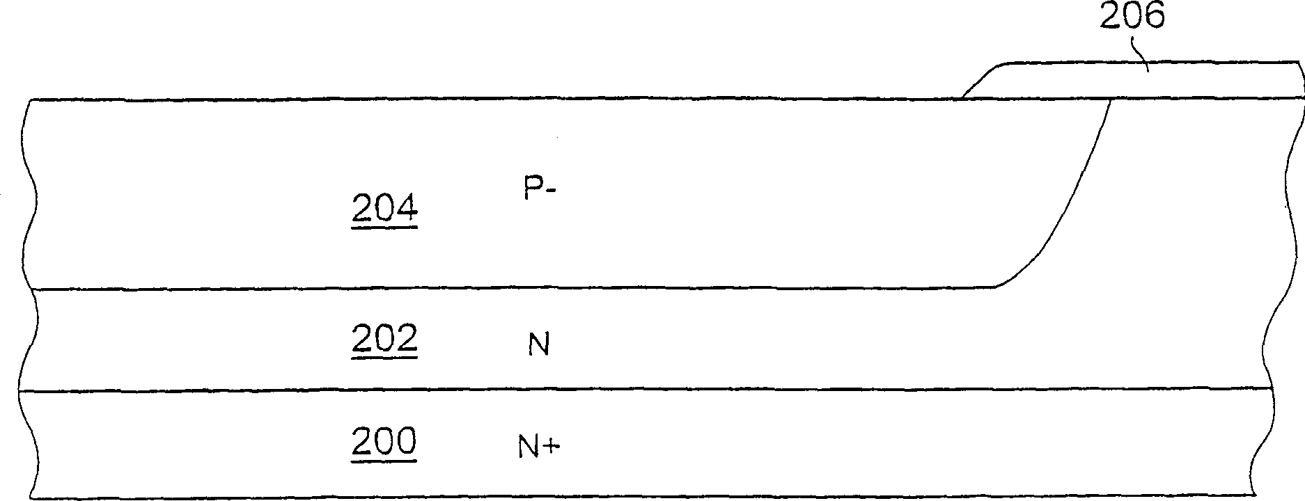
[0052] refer to figure 2 , shows trench MOSFET 219 with N-type epitaxial layer 202 formed on N+ substrate 200 . The N+ substrate 200 is a typical silicon substrate with a thickness ranging from 20 to 25 mils and a resistivity ranging from 0.005 to 0.01 Ω·cm. The N-type epitaxial layer 202 is also typical silicon, with a thickness ranging from 5 to 6 microns and a resistivity ranging from 0.18 to 0.25Ω·cm.

[0053] A trench 201 formed in the epitaxial layer is aligned with the gate oxide 210 and fills a polysilicon (ie, polysilicon) gate electrode 211 . The gate oxide 210 is typica...


PUM


Abstract

A trench MOSFET device and process for making the same are described. The trench MOSFET has a substrate of a first conductivity type, an epitaxial layer of the first conductivity type over the substrate, the epitaxial layer having a lower majority carrier concentration than the substrate, a plurality of trenches within the epitaxial layer, a first insulating layer, such as an oxide layer, lining the trenches, a conductive region, such as a polycrystalline silicon region, within the trenches adjacent to the first insulating layer, and one or more trench body regions and one or more termination body regions provided within an upper portion of the epitaxial layer, the termination body regions extending into the epitaxial layer to a greater depth than the trench body regions. Each trench body region and each termination body region has a first region of a second conductivity type, the second conductivity type being opposite the first conductivity type, and a second region of the second conductivity type adjacent the first region, the second region having a greater majority carrier concentration than the first region, and the second region being disposed above the first region and adjacent and extending to an outer wall of each of the plurality of trenches. A plurality of source regions of the first conductivity type are positioned adjacent the trenches within upper portions the trench body regions.

Description

technical field [0001] The present invention relates generally to microelectronic circuits, and more particularly to trench MOSFET devices. Background technique [0002] A DMOS (Double Diffused MOS) transistor is a type of MOSFET (Metal Oxide Semiconductor Field Effect Transistor) that uses diffusion to form a transistor region. DMOS transistors are commonly used as power transistors in high voltage power supply integrated circuits. DMOS transistors provide high current per unit area where low forward voltage drop is required. [0003] A typical discrete DMOS circuit includes two or more individual DMOS transistor cells configured in parallel. Individual DMOS transistor cells share a common drain contact, while their sources are all shorted together with metal and their gates are shorted together with polysilicon. Therefore, although this discrete DMOS circuit is constructed from a matrix of small transistors, it behaves as a single large transistor. [0004] A specific ...

Claims


Application Information

Patent Timeline
Patent Type & Authority Patents(China)
IPC IPC(8): H01L21/336H01L29/10H01L29/78
CPCH01L29/7813H01L29/1095H01L29/7811H01L21/18
Inventor 石甫渊苏根政
Owner GEN SEMICON
Why Eureka
Try Eureka