Display device and electron instrument

一种显示装置、电子仪器的技术,应用在照明装置、电固体器件、电路等方向,能够解决显示装置对比度下降、颜色污点等问题,达到提高对比度、提高视觉识别性的效果

Inactive Publication Date: 2005-10-26
MICROSOFT TECH LICENSING LLC
View PDF1 Cites 3 Cited by
  • Summary
  • Abstract
  • Description
  • Claims
  • Application Information

AI Technical Summary

Problems solved by technology

[0013] However, in the conventional display device, the colored light emitted from the light-emitting layer spreads not only to the viewer side but also to the periphery of the light-emitting layer (non-formation region of the light-emitting layer). The colored lights emitted by the light-emitting layer are mixed with each other, resulting in color stains and reducing the contrast of the display device

Method used


Image

  • Display device and electron instrument
  • Display device and electron instrument
  • Display device and electron instrument

Examples


Embodiment 1

[0075] Next, Embodiment 1 of the present invention will be described with reference to the drawings.

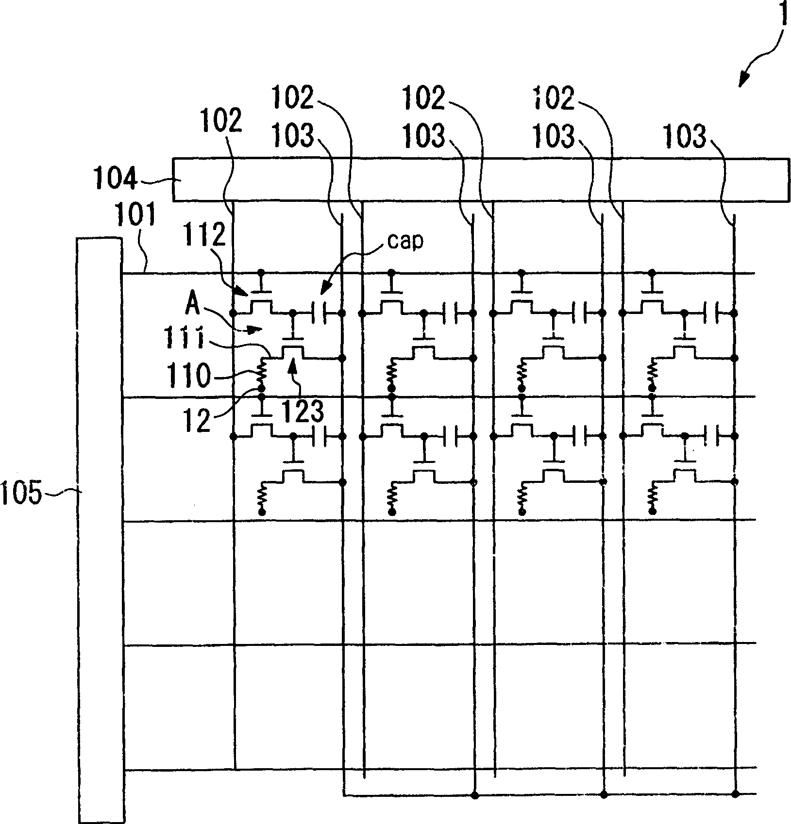
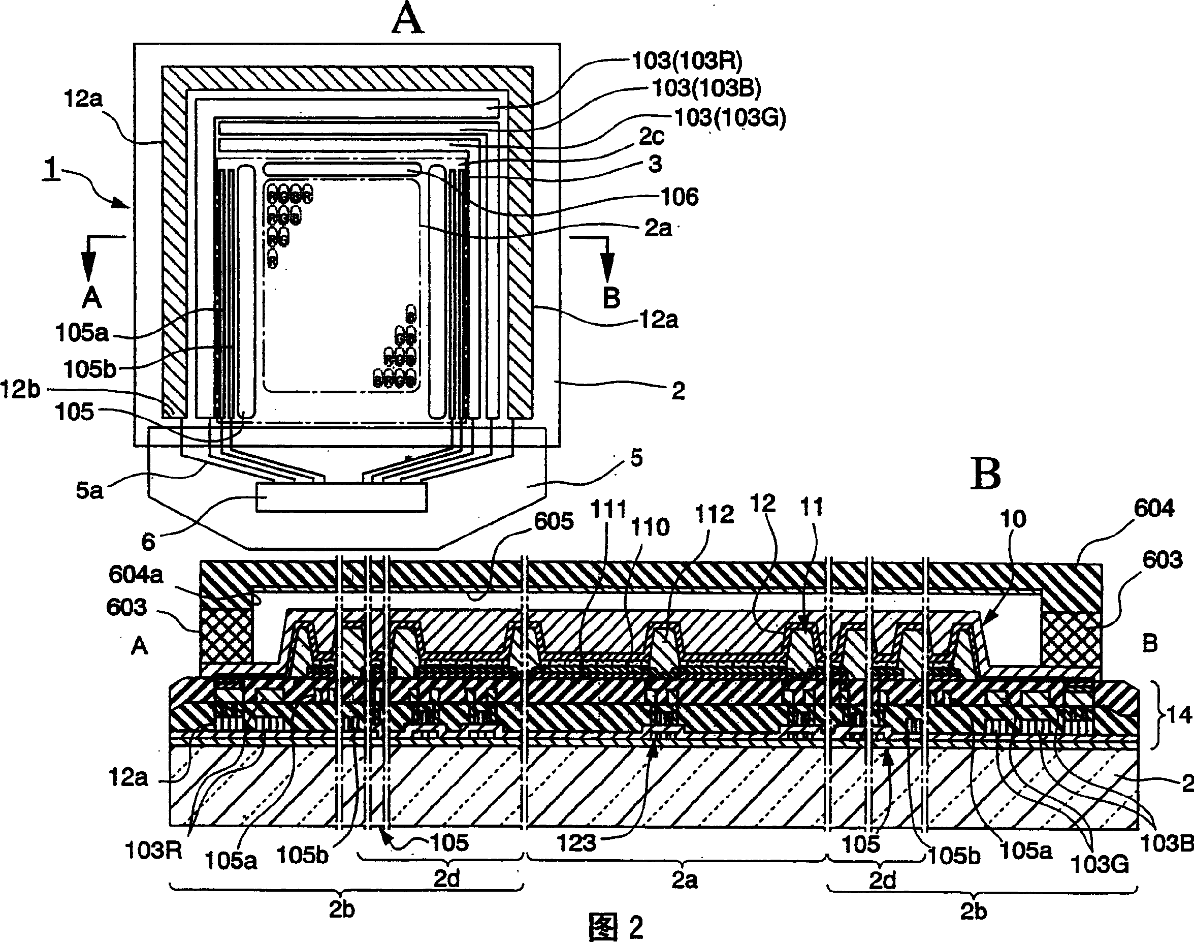
[0076] figure 1 A schematic plan view showing the wiring structure of the display device of this embodiment, and FIG. 2 shows a schematic plan view and a schematic cross-sectional view of the display device of this embodiment.

[0077] Such as figure 1 As shown, the display device 1 of this embodiment has a structure in which a plurality of scanning lines 101, a plurality of signal lines 102 extending in a direction intersecting the scanning lines 101, and a plurality of power supply lines 103 extending in parallel with the signal lines 102 are respectively provided. , and pixel regions A are provided near the intersections of the scanning lines 101 and the signal lines 102 .

[0078] On the signal line 102, a data-side driver circuit 104 having a shift register, a level shifter, a video line, and an analog switch is connected. In addition, a scanning line-side driver ci...

Embodiment 2

[0279] Next, Embodiment 2 of the present invention will be described with reference to the drawings.

[0280] Figure 21 It is a cross-sectional view showing the main part of the display device of the second embodiment.

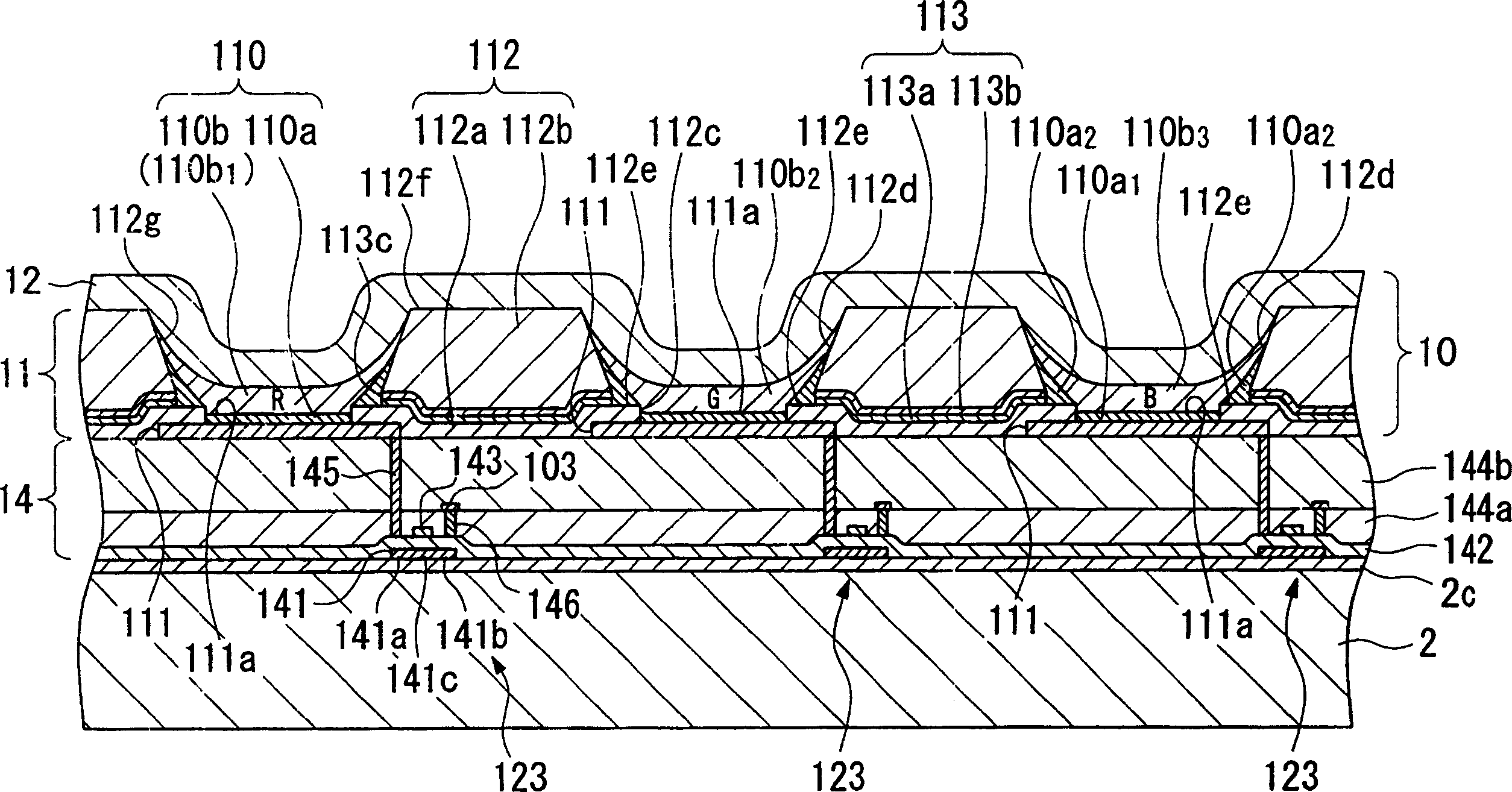
[0281] Such as Figure 21 As shown, the structure of the display device of this embodiment is that the circuit element portion 14 formed with circuits such as TFTs, the light emitting element portion 211 formed with a light emitting layer, and the cathode 12 are sequentially stacked on the substrate 2 .

[0282] In the display device of this embodiment, as in Embodiment 1, the light emitted from the functional layer 110 to the substrate 2 side passes through the circuit element portion 14 and the substrate 2, and is emitted to the lower side of the substrate 2 (observation the other side), and the light emitted from the functional layer 110 to the opposite side of the substrate 2 is reflected by the cathode 12, passes through the circuit element part 14 and...

Embodiment 3

[0296] Next, Embodiment 3 of the present invention will be described with reference to the drawings.

[0297] Figure 22 It is a sectional view showing the main part of the display device of the third embodiment.

[0298] Such as Figure 22 As shown, the structure of the display device of this embodiment is that the circuit element portion 14 formed with circuits such as TFTs, the light emitting element portion 311 formed with a light emitting layer, and the cathode 12 are sequentially stacked on the substrate 2 .

[0299] In the display device of this embodiment, as in the first and second embodiments, the light emitted from the functional layer 110 to the substrate 2 side passes through the circuit element portion 14 and the substrate 2, and is emitted to the lower side of the substrate 2. (observer side), and the light emitted from the functional layer 110 to the opposite side of the substrate 2 is reflected by the cathode 12, passes through the circuit element part 14 an...


PUM


Abstract

A display apparatus is provided that prevents shortening of the life of the luminescent elements and has a superior contrast ratio. The display apparatus is composed by forming a plurality of luminescent elements on a substrate and providing bank sections between each of the luminescent elements. The bank sections are formed from a first bank layer located on the side of the substrate and a second bank layer formed on the first bank layer. A light blocking layer is then provided between the first bank layer and the second bank layer.

Description

technical field [0001] The present invention relates to a display device and an electronic instrument. Background technique [0002] In recent years, light-emitting materials such as organic fluorescent materials have been made into inks, and according to the inkjet method of ejecting the ink (composition) on a base material, a method of patterning the light-emitting materials has been carried out, and sandwiching between the anode and the cathode has been carried out. Development of a color display device having a structure of a light-emitting layer made of this light-emitting material, particularly an organic EL (electroluminescence) display device using an organic light-emitting material as a light-emitting material (refer to Patent Document 1 (JP-A-10-12377 No. Gazette)). [0003] Therefore, a conventional display device (organic EL display device) will be described with reference to the drawings. [0004] Figure 31 It is a schematic cross-sectional view showing a mai...

Claims


Application Information

Patent Timeline
Patent Type & Authority Patents(China)
IPC IPC(8): H05B33/22H01L27/32H01L51/50H01L51/52H05B33/12
CPCH01L27/3246H01L51/5284H01L27/3211H10K59/35H10K59/122H10K59/8792H05B33/22H10K50/865
Inventor 关俊一
Owner MICROSOFT TECH LICENSING LLC
Why Eureka
Try Eureka