Static relay and communication device using static relay

A relay and electrostatic technology, applied in the field of electrostatic relays, can solve the problems of increased contact resistance between contacts, decreased contact force between contacts, and reduced electrostatic attraction, etc., to achieve reduced insertion loss, easy processing, and good high-frequency characteristics Effect

Inactive Publication Date: 2006-04-05
ORMON CORP
View PDF0 Cites 0 Cited by
  • Summary
  • Abstract
  • Description
  • Claims
  • Application Information

AI Technical Summary

Problems solved by technology

[0011] However, if the electrostatic microrelay is miniaturized, the electrode area of ​​the movable electrode and the fixed electrode is also reduced, so the electrostatic attraction acting between the electrodes becomes smaller, and the contact force between the contacts decreases.
As a result, the contact resistance between the contacts increases and the insertion loss also increases
[0012] In this way, in the existing electrostatic microrelays of such a structure, because there is a trade-off relationship between the resistance of the signal line and the contact force between the contacts, miniaturization of the electrostatic microrelay is not necessarily related to improving the insertion loss of the electrostatic microrelay.

Method used


Image

  • Static relay and communication device using static relay
  • Static relay and communication device using static relay
  • Static relay and communication device using static relay

Examples


Embodiment Construction

[0065] DETAILED DESCRIPTION OF THE PREFERRED EMBODIMENTS Preferred embodiments of the present invention will be described in detail below with reference to the accompanying drawings.

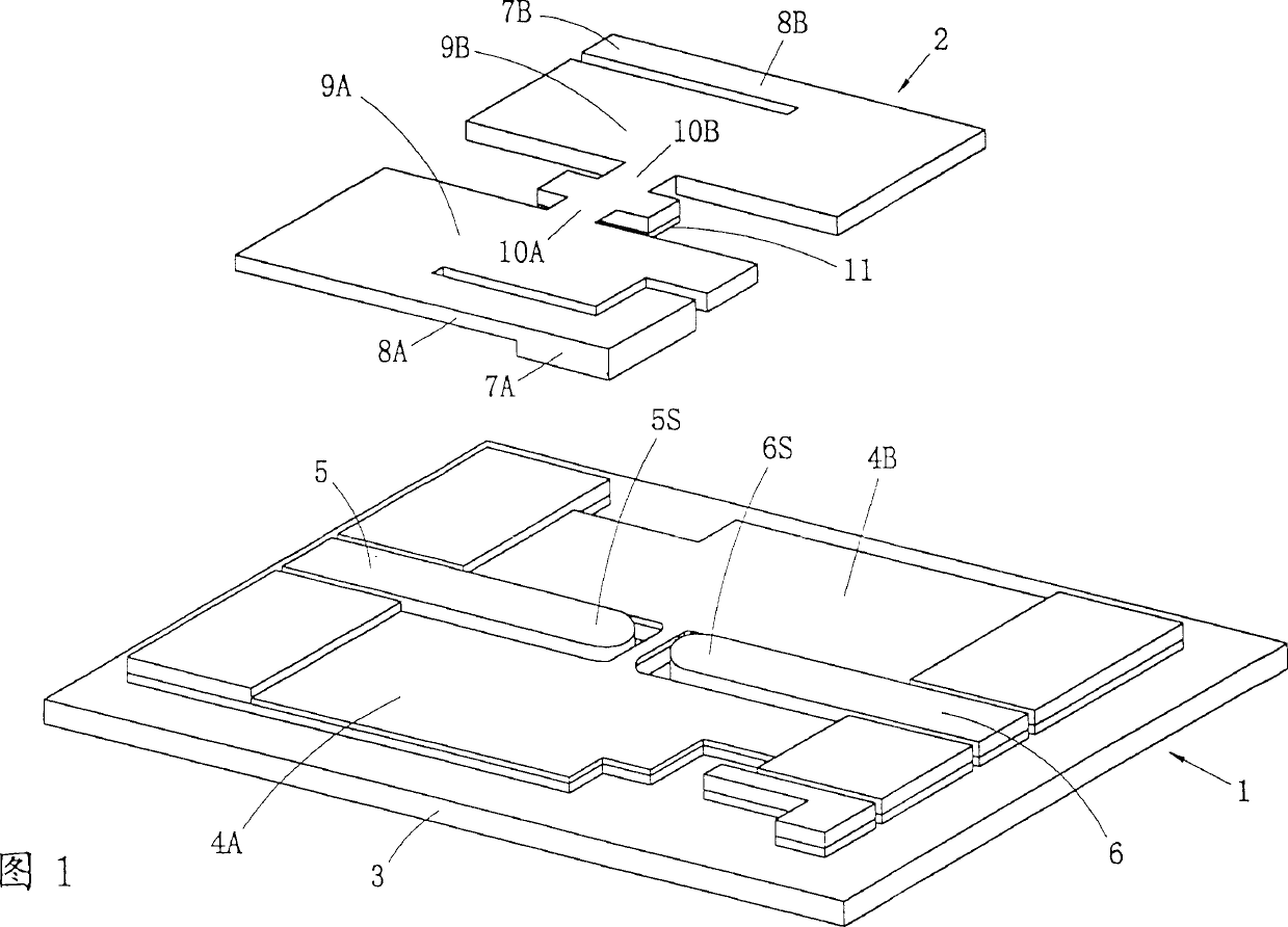
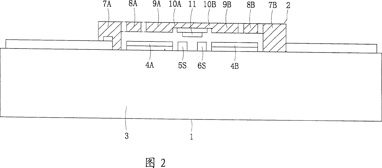
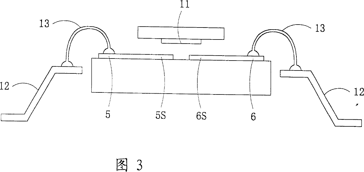
[0066] Fig. 4 is an exploded oblique view of the structure of an electrostatic micro-relay according to an embodiment of the present invention. Fig. 5 is a step-by-step sectional view taken along line X-X in Fig. 4 . This electrostatic micro-relay is mainly made of fixed substrate 20, movable substrate 40 and cap 50, and movable substrate 40 is installed on the top of fixed substrate 20 for integration, and the top of fixed substrate 20 and movable The substrate 40 is sealed between the fixed substrate 20 and the cap 50 . FIG. 6 is a perspective view seen from the back side of this fixing substrate 20, and FIG. 7 is a perspective view seen from the back side of the cap 50. As shown in FIG.

[0067] As shown in FIG. 4, the above-mentioned fixed substrate 20 is a substrate in which fixed electro...


PUM


Abstract

Fixed contacts (23A, 24A) are provided on the upper surface of a silicon substrate (21). Signal lines (23, 24) electrically continuous with the fixed contacts (23A, 24A) are provided so as to pass through a silicon substrate (21) from the obverse surface to the reverse surface thereof. Bumps (32, 33) electrically continuous with the signal lines (23, 24) are provided on the reverse surface of the silicon substrate (21). A fixed electrode (22) is provided on both sides of the fixed contacts (23A, 24A). Wiring conductors (30, 31) electrically continuous with the fixed electrode (22) are provided so as to pass through the silicon substrate (21) from the obverse surface to the reverse surface thereof. Bumps (34, 35) electrically continuous with the wiring conductors (30, 31) are provided on the reverse surface of the silicon substrate (21). Through holes (26, 27) of the silicon substrate (21) through which the signal lines (23, 24) are passed and through holes (28, 29) of the silicon substrate (21) through which the wiring conductors (30, 31) are passed are hermetically sealed by a movable substrate (40) or a cap (50).

Description

technical field [0001] The present invention relates to an electrostatic relay in which a movable contact is opened and closed by electrostatic attraction and a communication device using the relay. In particular, it relates to a small electrostatic micro-relay made by micromachining technology. Background technique [0002] As an electrostatic microrelay, we have hitherto known the relay disclosed in the paper "Micro Machined Relay for High Frequency" (Y. Komura, et al.). FIG. 1 is an exploded perspective view showing the structure of this electrostatic microrelay. In addition, the sectional view of FIG. 2 is a figure which schematically shows this structure. This electrostatic microrelay can be roughly divided into two parts: a fixed substrate 1 and a movable substrate 2 . On the fixed substrate 1, two signal lines 5, 6 are formed on the substrate 3, and the ends of the respective signal lines 5, 6 face each other with a small gap therebetween, forming fixed contacts 5S...

Claims


Application Information

Patent Timeline
Patent Type & Authority Patents(China)
IPC IPC(8): H01H59/00H01P1/10B81B3/00B81C3/00H01H1/20
CPCH01H59/0009H01H1/20H01H59/00
Inventor 藤井充坂田稔积知范佐藤正武
Owner ORMON CORP
Why Eureka
Try Eureka