Source/drain ion injecting method for lowering defect on substrate

An ion implantation and substrate technology, which is applied in semiconductor/solid-state device manufacturing, electrical components, circuits, etc., and can solve problems such as increasing manufacturing costs, affecting the performance of other components, and dislocation defects.

Inactive Publication Date: 2006-06-14
MACRONIX INT CO LTD
View PDF1 Cites 0 Cited by
  • Summary
  • Abstract
  • Description
  • Claims
  • Application Information

AI Technical Summary

Problems solved by technology

For example, in R.Troutman, "Latch-Up in CMOSTechnology: The Problem and Its Cure." Kluwer Academic, Norwell, Mass. (1986) document, it is proposed to carry out high doping concentration (1E14--1E16atom / cm 2 ) ion implantation method to reduce the latch-up phenomenon; however, although the ion implantation method with high doping concentration can achieve the purpose of reducing the latch-up phenomenon, the ion implantation manufacturing method with high dopant concentration will cause substrate defects, such as bit Dislocation defect, etc.
[0003] In addition, it was also proposed to use trench isolation (Trench Isolation) to solve the latch-up phenomenon, as described in US Patent No. 5,937,288, but when digging trenches, it will also cause substrate defects
[0004] In addition, regarding the manufacturing method of the source and drain of Metal-Oxide-Semiconductor (MOS) components, it is usually formed by ion implantation with high doping concentration, so there will also be the above-mentioned substrate The problem of defects occurs, which seriously affects the reliability of the product (reliability)
[0005] In addition, although traditional thermal manufacturing methods of high temperature (>1000°C) or rapid temperature rise and fall (temperature rise and fall rate>50°C / sec) can be used to eliminate substrate defects and achieve thermal activation (thermal activation), however, this High-temperature manufacturing methods can affect the performance of other components, and rapid ramp-up and heating manufacturing methods are usually additional manufacturing methods, thus increasing manufacturing costs

Method used


Image

  • Source/drain ion injecting method for lowering defect on substrate
  • Source/drain ion injecting method for lowering defect on substrate
  • Source/drain ion injecting method for lowering defect on substrate

Examples


Embodiment Construction

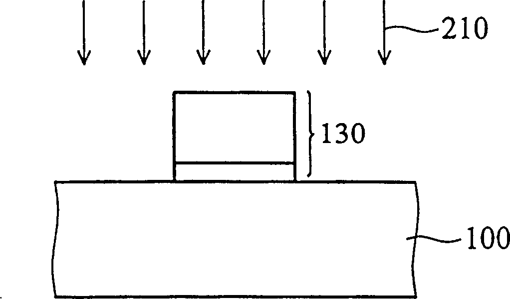
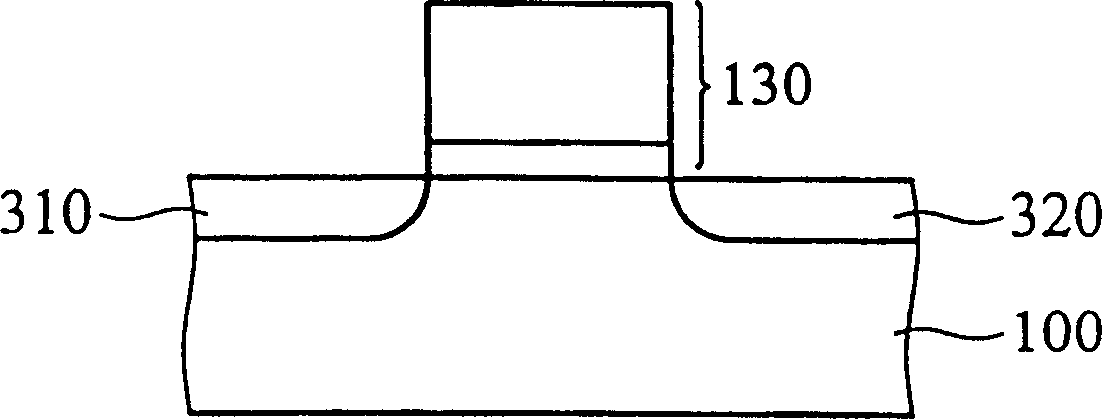
[0014] Embodiments of the present invention will be described below using the cross-sectional views of the manufacturing method shown in FIGS. 1-3. It should be noted here that although the present embodiment takes the MOS manufacturing method as an example, it does not limit the present invention. That is to say, the present invention is applicable to ion implantation manufacturing methods of any semiconductor products (such as CMOS, various memories, etc.).

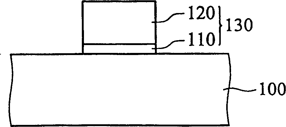
[0015] First, please refer to figure 1 , providing a substrate 100 such as a silicon substrate (Si substrate). Then, using thermal oxidation, chemical vapor deposition or chemical oxidation, etc., to form a SiO 2 A gate oxide layer (not shown) of the first layer, and then a gate layer (not shown), such as a polysilicon layer, is deposited by chemical vapor deposition. Then, a patterned gate oxide layer 110 and a patterned gate layer 120 are formed through a photolithography process to form a gate structure 130 .

[...


PUM


Abstract

The invention relates to a method for ion implantation of high doping concentration for reducing substrate defects. A high concentration (1E14-1E16 atom / cm 2 ) ion implantation program, wherein the ion implantation program includes a low ion beam current, the range of the low ion beam current is 1-7mA. Accordingly, the present method utilizes the low ion beam current to reduce substrate defects produced by the ion implantation process.

Description

technical field [0001] The invention relates to a method for manufacturing a semiconductor integrated circuit (integrated circuit; IC), in particular to an ion implantation method for reducing substrate defects with high doping concentration. Background technique [0002] In the use of Complementary Metal-Oxide Semiconductor (CMOS) devices, there is a shortcoming of the so-called latch-up phenomenon, and many methods to solve the latch-up phenomenon have been proposed so far. For example, in R.Troutman, "Latch-Up in CMOSTechnology: The Problem and Its Cure." Kluwer Academic, Norwell, Mass. (1986) document, it is proposed to carry out high doping concentration (1E14--1E16atom / cm 2 ) ion implantation method to reduce the latch-up phenomenon; however, although the ion implantation method with high doping concentration can achieve the purpose of reducing the latch-up phenomenon, the ion implantation manufacturing method with high dopant concentration will cause substrate defec...

Claims


Application Information

Patent Timeline
Patent Type & Authority Patents(China)
IPC IPC(8): H01L21/265H01L21/324
Inventor 王嗣裕苏俊联
Owner MACRONIX INT CO LTD
Why Eureka
Try Eureka