Semiconductor memory device
A storage device and semiconductor technology, which is applied in the fields of semiconductor devices, information storage, and semiconductor/solid-state device manufacturing, etc., can solve problems such as a decrease in the qualification rate and an increase in the number of manufacturing processes.
- Summary
- Abstract
- Description
- Claims
- Application Information
AI Technical Summary
Problems solved by technology
Method used
Image

Examples
Embodiment approach 1
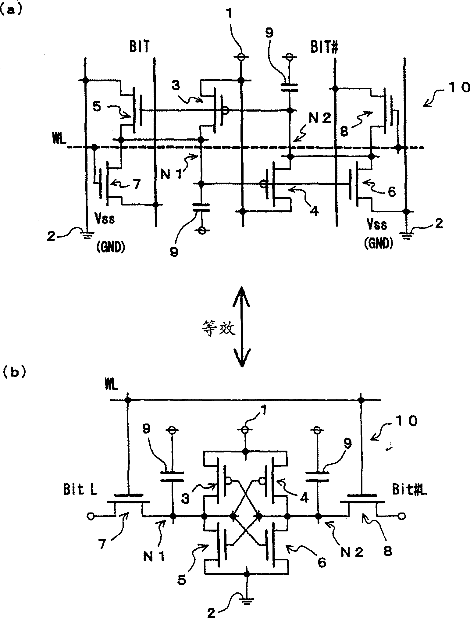
[0059] figure 1 (a) and (b) are circuit diagrams of a typical all-CMOS type memory cell of a type in which charge capacity is added to a cell node for countermeasures against soft errors. figure 1 The two circuits shown in (a) and (b) are equivalent circuits, in figure 1 In (a), each component is arranged corresponding to the actual structure of the horizontally long memory cell, and on the other hand, in figure 1 In (b), each component is arranged according to the principle of simplifying and clarifying the circuit diagram.
[0060] The memory cell 10 has a general six-transistor unit structure, and has a first p-type large-capacity load transistor (hereinafter referred to as the first load transistor) 3 and a second p-type large-capacity load transistor (hereinafter referred to as the second load transistor) 4 as transistors. , 1n-type large-capacity driving transistor (hereinafter referred to as the first driving transistor) 5, 2n-type large-capacity driving transisto...
Embodiment approach 2
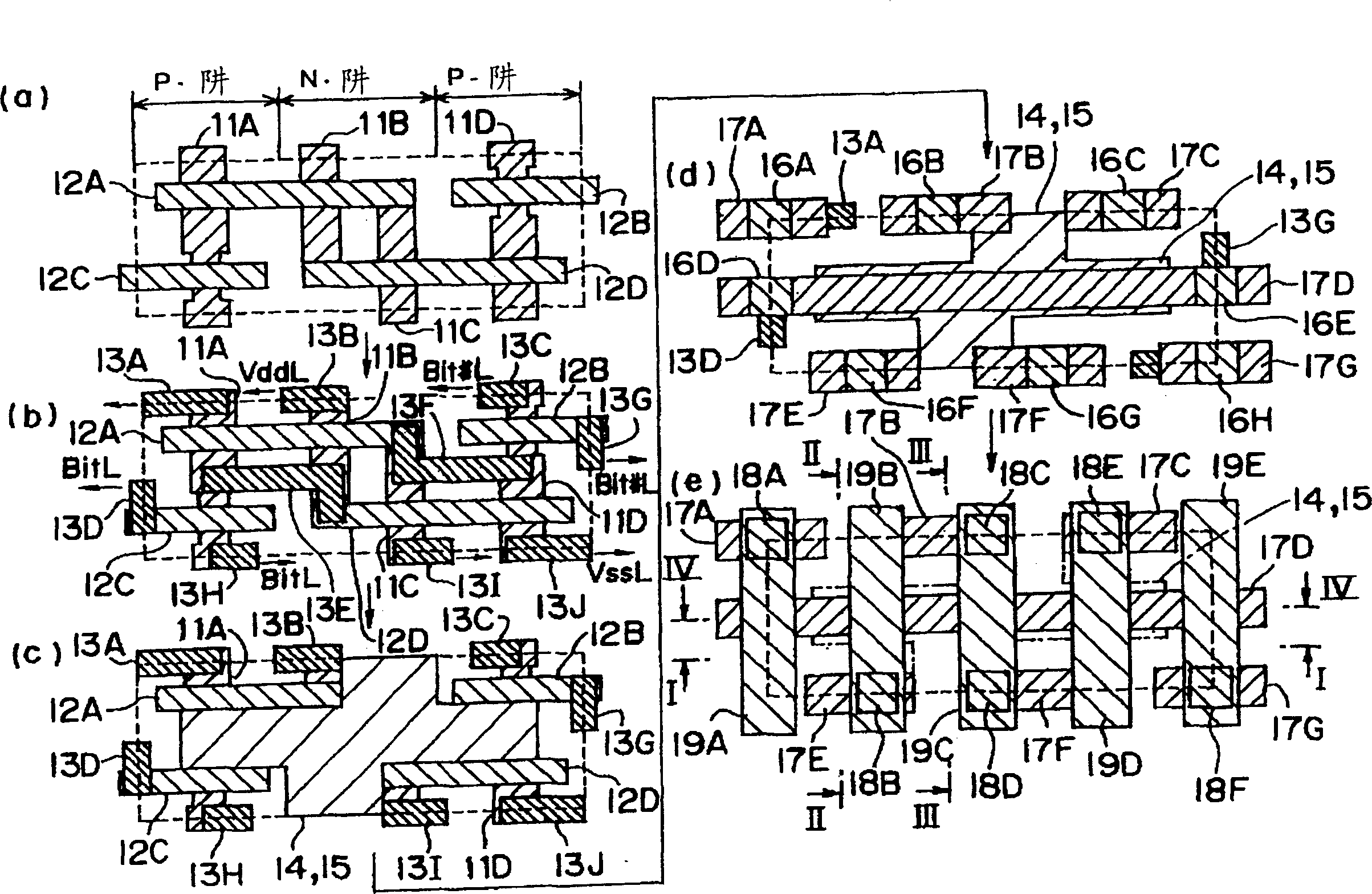
[0100] Figure 8 is a plan view of each stage of the manufacturing process of the full CMOS memory cell according to Embodiment 2 of the present invention, Figure 8 (a) and (b) respectively with figure 2 (c) and (e) correspond. In the first embodiment described above, the case where the power supply voltage (Vdd) is applied to the conductive film 15 constituting the charging capacity body is described, but the present invention is not limited to this, and a ground voltage may be applied to the conductive film constituting the charging capacity body. (Vss), the potential of the conductive film is equal to the potential of the sources of the first and second driving transistors 5 and 6. In this case, if Figure 8 As shown in (a), a sufficient margin can be maintained between the conductive film 35 and the mosaic wiring 13B, 13C, 13D, 13G, 13H, and 13I connected to each power supply voltage line or bit line without contact. On the other hand, the interval between the conduc...
Embodiment approach 3
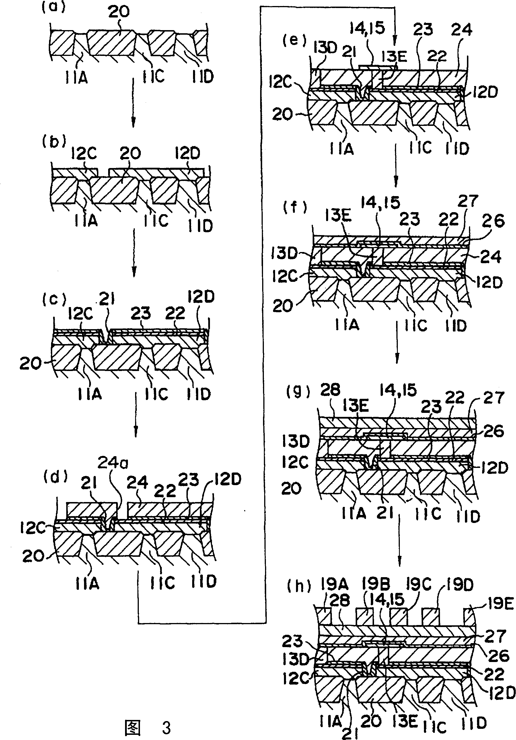
[0107] Figure 13 (a) to (f) are diagrams showing respective states during formation of cell nodes and charging capacity bodies included in the memory cell according to Embodiment 3 of the present invention. In this Embodiment 3, the difference from the above-mentioned Embodiment 1 is that, after forming the trench for wiring and the concave portion communicating with the trench for wiring, they are buried simultaneously. A technique for forming cell nodes and charge capacitors (so-called dual damascene processing). exist Figure 13 In the state shown in (a), the etching stopper film 23 is formed after the active layers 11A, 11B, 11C, and 11D are formed, as in the case of Embodiment 1 described above. From this state, such as Figure 13 As shown in (b), the planarization insulating film 24 is formed on the entire surface, and then the etching stopper layer 41 and the planarization insulating film 42 are deposited.
[0108] Thereafter, the planarization insulating film 42 o...
PUM
 Abstract
Description
Claims
Application Information
 - R&D
- Intellectual Property
- Life Sciences
- Materials
- Tech Scout
- Unparalleled Data Quality
- Higher Quality Content
- 60% Fewer Hallucinations
Browse by: Latest US Patents, China's latest patents, Technical Efficacy Thesaurus, Application Domain, Technology Topic, Popular Technical Reports.
© 2025 PatSnap. All rights reserved.Legal|Privacy policy|Modern Slavery Act Transparency Statement|Sitemap|About US| Contact US: help@patsnap.com