Method for producing embedded DRAM unit array with selected transistor

A technology for selecting transistors and cell arrays, applied in information storage, static memory, digital memory information, etc., can solve the problems of conflicting process requirements, difficulty in reliability, and difficulty in producing high-performance memory devices, so as to improve performance, The effect of reducing the size

Inactive Publication Date: 2006-10-18
萧正杰
View PDF9 Cites 0 Cited by
  • Summary
  • Abstract
  • Description
  • Claims
  • Application Information

AI Technical Summary

Problems solved by technology

It is very difficult to achieve ideal yield and certain reliability with such complicated process technology at present.
Moreover, due to the conflicting process requirements of logic circuits and memory devices, it is difficult to produce high-performance memory devices with current embedded manufacturing technologies.
None of the current embedded manufacturing technologies have proven successful

Method used


Image

  • Method for producing embedded DRAM unit array with selected transistor
  • Method for producing embedded DRAM unit array with selected transistor
  • Method for producing embedded DRAM unit array with selected transistor

Examples


Embodiment Construction

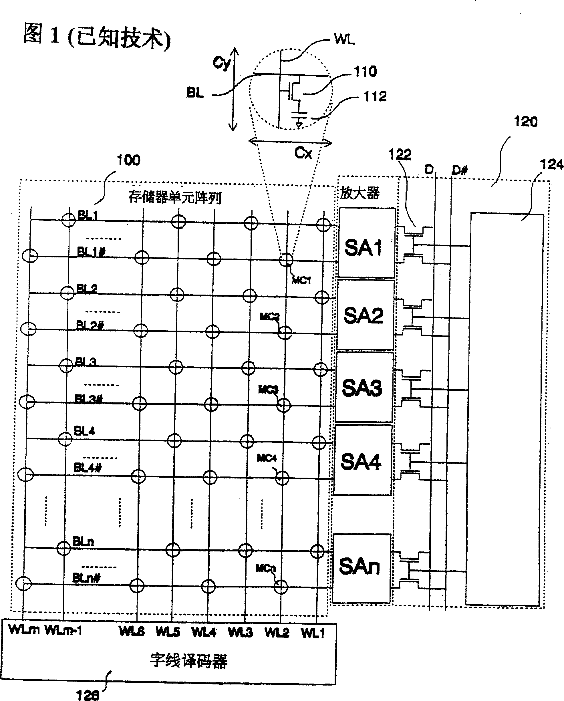
[0056] Before describing the present invention, the existing semiconductor memory device is firstly introduced, which is helpful for understanding the present invention.

[0057] Fig. 1 shows the structure of the memory cell array of the existing DRAM in two ways of electronic circuit and topological diagram. The memory cell array 100 includes several pairs of bit lines BL1, BL1#, BL2, BL2#, BL3, BL3#, . . . , BLn, BLn# (n is an integer) parallel to each other, and several pairs of The word lines WL1 , WL2 . . . WLm (m is an integer) cross vertically. At these intersections, memory cells MC1, MC2, . . . , MCn are respectively arranged. The memory cells are represented by individual circles in the memory cell array 100 shown in FIG. 1 . Each memory cell includes a field effect switching transistor 110 and a memory cell capacitor 112 . The bit line BL is connected to the drain of the transistor 110 . The gate electrode of the transistor 110 is connected to the word line WL. ...


PUM


Abstract

A dynamic random access memory disclosed by the invention adopts a multi-dimensional bit line structure to solve the long-standing problem of excessively dense distribution intervals of memory devices. Improvements in decoder design have further reduced the overall area of ​​such memory devices. The invention also discloses a new memory access method, which can make external users completely unaware of the data update operation performed inside the memory. By using this memory structure, DRAM with higher performance can be manufactured without reducing memory density. Moreover, the memory requirements for system support are greatly simplified.

Description

technical field [0001] The present invention relates to high performance semiconductor memory devices, and more particularly to embedded memory devices with primary bit lines connected in different design directions. Background technique [0002] Generally, DRAM (Dynamic Random Access Memory) is considered as a high-density, low-cost, but low-performance memory device. DRAMs currently on the market have always exhibited low performance compared to other types of semiconductor memory devices, such as static random access memory (SRAM). The density of DRAM is improving rapidly, with each generation of devices being more than twice as integrated as the previous generation. Relying on ultra-fine process technology and improving the structure of memory cells, although DRAM can achieve a high degree of integration, the speed of improvement in performance of DRAM is quite slow, resulting in a performance gap between memory devices and logic devices. . At present, many new method...

Claims


Application Information

Patent Timeline
Patent Type & Authority Patents(China)
IPC IPC(8): G11C11/00
Inventor 萧正杰
Owner 萧正杰
Why Eureka
Try Eureka