Method for forming self alignment contact window

A self-aligned contact and contact area technology, applied in the direction of electrical components, semiconductor/solid-state device manufacturing, semiconductor devices, etc., can solve problems such as short circuits

Inactive Publication Date: 2007-03-07
MACRONIX INT CO LTD
View PDF6 Cites 0 Cited by
  • Summary
  • Abstract
  • Description
  • Claims
  • Application Information

AI Technical Summary

Problems solved by technology

Since the dielectric layer 32 and the buffer layer 30 are made of silicon oxide, the etching gas or etching solution used in the etching of the contact window or the cleaning of the contact window will also damage the buffer layer 30 located between the gate stack structure 14 and the sidewall layer 22 , and the metal layer 28 is exposed, resulting in a short circuit between the metal layer 28 and the contact metal filled in the opening 34

Method used


Image

  • Method for forming self alignment contact window
  • Method for forming self alignment contact window
  • Method for forming self alignment contact window

Examples


Embodiment Construction

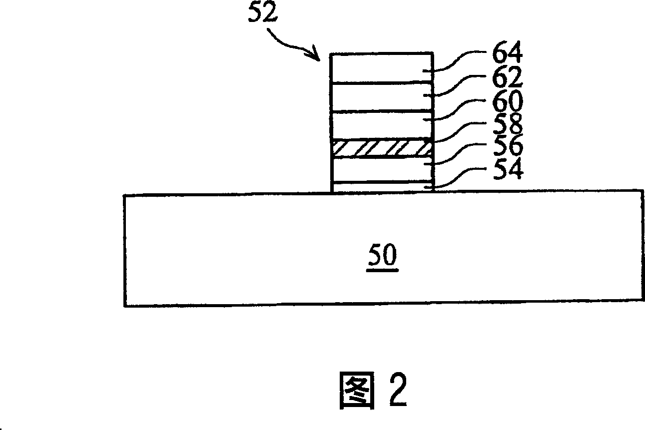
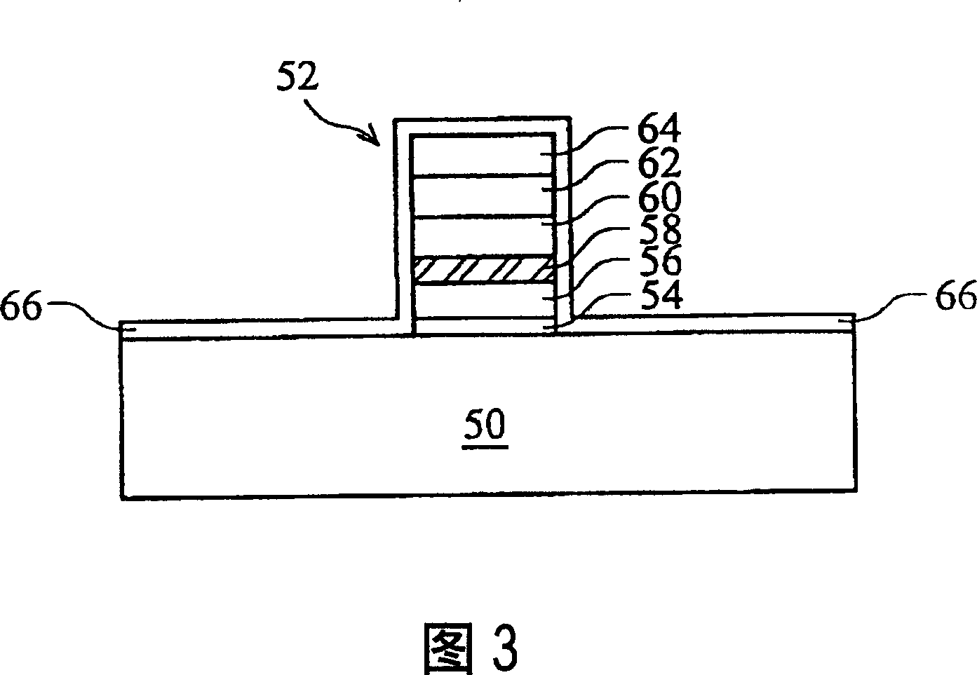
[0044] 2-8 show an embodiment of the self-aligned contact forming method of the present invention. Referring to FIG. 2 , a semiconductor substrate 50 is provided, and a gate stack structure 52 is formed on the semiconductor substrate 50 , and a source / gate pair and a channel can be formed in the semiconductor substrate at this stage as required. The stacked gate structure 52 includes a gate insulating layer 54 , a second metal layer 60 and an interlayer dielectric layer 58 formed between the first metal layer 56 and the second metal layer 60 to provide electrical insulation between the two metal layers. In one embodiment, the gate insulating layer 54 is made of silicon oxide, the first metal layer 56 includes polysilicon, and the second metal layer 60 includes a refractory metal layer. In another embodiment, the third metal layer 62 formed on the second metal layer 60 including polysilicon includes tungsten suicide. The third metal layer 62 may enhance the conductivity of the...


PUM


Abstract

The invention is a self-aligning contact window forming method, including: arranging at least a grid-superposed structure on a semiconductor substrate; forming a first dielectric layer on them; forming a second dielectric layer on the first one, where the second one has etching selectivity relative to the first one; etching the second dielectric layer to expose the first dielectric layer formed on the top surface of the grid- superposed structure and at the upper part of partial side wall of the grid-superposed structure; eliminating the exposed dielectric layer; and forming a third dielectric layer on the side wall of the grid-superposed structure.

Description

technical field [0001] The invention relates to a method for manufacturing a semiconductor integrated circuit, in particular to a method for forming a self-aligned contact window in the semiconductor integrated circuit. Background technique [0002] A field effect transistor (FET) generally includes: an insulating layer formed on a semiconductor substrate, a polysilicon gate formed on the insulating layer, a pair of source / drain regions formed in the semiconductor substrate, and a gate electrode formed on the gate A channel region under the insulating layer and separated by the source / drain region. In the field effect transistor manufacturing process, traditional flash memory technology includes the metallization process of the source / gate electron pair of the circuit. The metallization process includes disposing a patterned masking layer on the semiconductor substrate and exposing source or drain regions formed in the semiconductor substrate. In particular, openings are f...

Claims


Application Information

Patent Timeline
Patent Type & Authority Patents(China)
IPC IPC(8): H01L21/28H01L21/336H01L21/82
Inventor 郑培仁
Owner MACRONIX INT CO LTD
Why Eureka
Try Eureka