Semiconductor device, manufacturing method thereof, and electronic device

A manufacturing method and semiconductor technology, applied in the direction of semiconductor devices, semiconductor/solid-state device manufacturing, electric solid-state devices, etc., can solve the problems of gate and source/drain breakdown voltage reduction, so as to avoid breakdown voltage reduction, performance and good The effect of rate improvement, performance improvement and yield rate improvement

Active Publication Date: 2021-02-26
SEMICON MFG INT (SHANGHAI) CORP +1
View PDF5 Cites 0 Cited by
  • Summary
  • Abstract
  • Description
  • Claims
  • Application Information

AI Technical Summary

Problems solved by technology

[0006] Aiming at the deficiencies of the prior art, the present invention proposes a method for manufacturing a semiconductor device, which can overcome the decrease in the breakdown voltage between the gate and source / drain caused by the removal of the inversion contact etch stop layer at the top of the gate spacer The problem

Method used


Image

  • Semiconductor device, manufacturing method thereof, and electronic device
  • Semiconductor device, manufacturing method thereof, and electronic device
  • Semiconductor device, manufacturing method thereof, and electronic device

Examples


Embodiment 1

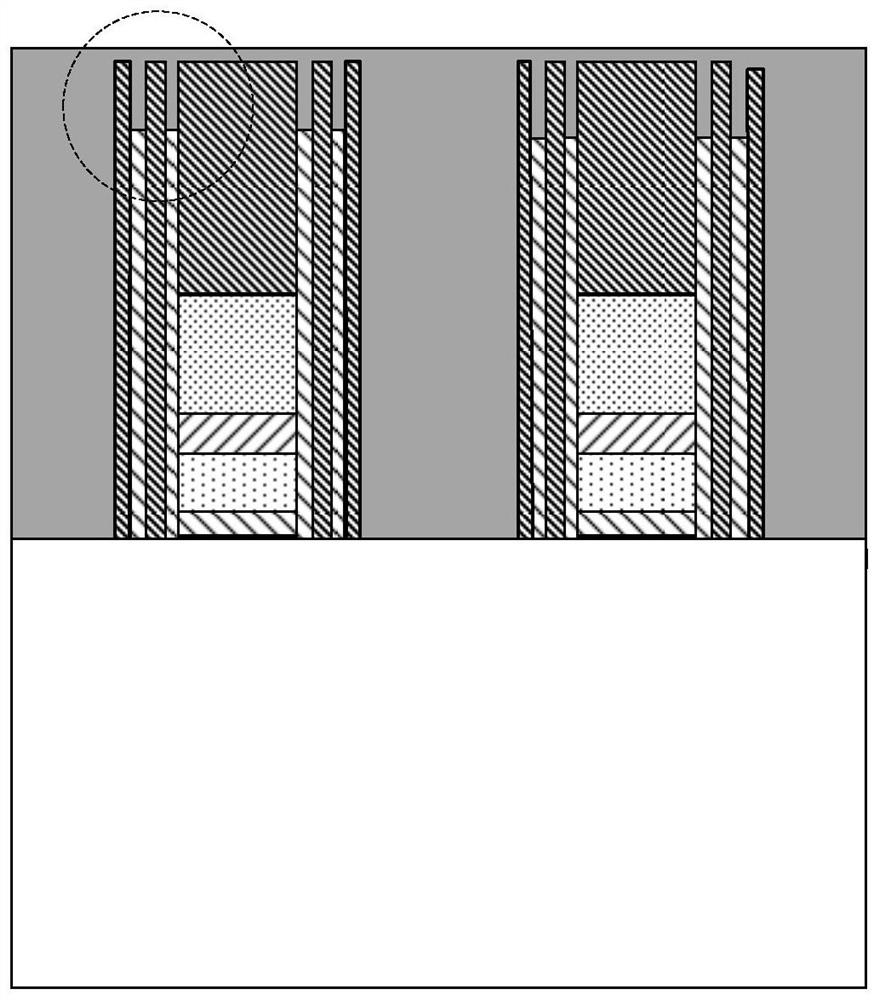
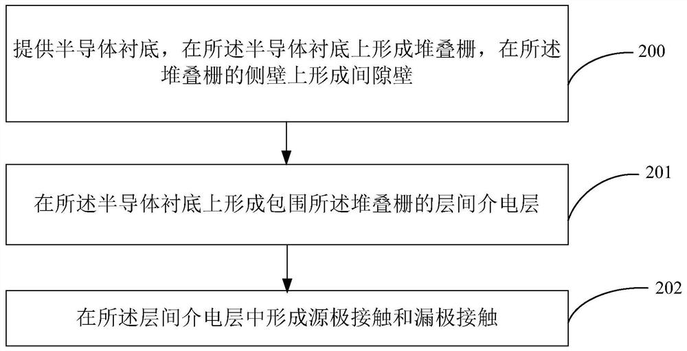
[0054] The following will refer to 3A to 17A as well as 3B to 17B A method for fabricating a semiconductor device according to an embodiment of the present invention is described in detail, wherein 3A to 17A A cross-sectional view along the direction of the active region of the semiconductor device obtained by sequentially implementing the steps of the method for fabricating a semiconductor device according to an embodiment of the present invention; 3B to 17B A cross-sectional view of the semiconductor device along the direction of the isolation structure obtained by sequentially performing various steps in the method for fabricating a semiconductor device according to an embodiment of the present invention is shown.

[0055] In this embodiment, the fabrication method of the semiconductor device proposed by the present invention is described in detail by taking the fabrication of the source-drain contacts of the NOR memory as an example. Please refer to the above drawing...

Embodiment 2

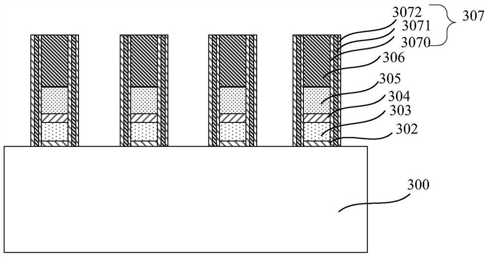
[0101] The present invention also provides a semiconductor device fabricated by the above method, such as Figure 17A and Figure 17B As shown, the semiconductor device includes: a semiconductor substrate 300, on which a stacked gate is formed, and a spacer 307A is formed on the sidewall of the stacked gate 300; on the semiconductor substrate 300 An interlayer dielectric layer surrounding the stacked gate is formed; a source contact 315A and a drain contact 315B are formed in the interlayer dielectric layer; wherein, the top region of the spacer 307A is entirely connected to the interlayer The dielectric layer is composed of materials with etch selectivity.

[0102] The isolation structure 301 in the semiconductor substrate 300 may be a shallow trench isolation (STI) structure or a localized silicon oxide (LOCOS) isolation structure, which may be formed by methods commonly used in the art to define and separate active regions. As an example, a shallow trench isolation (STI) ...

Embodiment 3

[0108] Yet another embodiment of the present invention provides an electronic device including a semiconductor device and an electronic component connected to the semiconductor device. Wherein, the semiconductor device includes: a semiconductor substrate, a stacked gate is formed on the semiconductor substrate, and a spacer is formed on a sidewall of the stacked gate; and a space surrounding the stack is formed on the semiconductor substrate an interlayer dielectric layer of the gate; a source contact and a drain contact are formed in the interlayer dielectric layer; wherein, the top region of the spacer is entirely composed of etch selectivity with the interlayer dielectric layer material composition.

[0109] Wherein, the semiconductor substrate can be at least one of the following materials: Si, Ge, SiGe, SiC, SiGeC, InAs, GaAs, InP or other III / V compound semiconductors, and also includes multilayers composed of these semiconductors The structure or the like may be silico...


PUM


Abstract

The present invention provides a semiconductor device, a manufacturing method thereof, and an electronic device. The manufacturing method includes: providing a semiconductor substrate, forming a stacked gate on the semiconductor substrate, and forming a spacer on a side wall of the stacked gate; An interlayer dielectric layer surrounding the stacked gate is formed on the semiconductor substrate; a source contact and a drain contact are formed in the interlayer dielectric layer; wherein, the top region of the spacer is entirely composed of the The interlayer dielectric layer is made of etch-selective material. The manufacturing method can overcome the problem of the reduction of the breakdown voltage between the gate and the source / drain caused by the removal of the inversion contact etch stop layer on the top of the gate spacer. The semiconductor device and electronic device have similar advantages.

Description

technical field [0001] The present invention relates to the technical field of semiconductors, and in particular, to a semiconductor device, a manufacturing method thereof, and an electronic device. Background technique [0002] With the popularity of portable personal devices, the demand for memory has further increased, and the research on memory technology has become an important direction of information technology research. In order to better improve the storage density and the reliability of data storage, the focus of research and development has gradually become Focus on non-volatile memory (NVM, non-volatile memory). NOR (NOR-type electronic logic gate) type flash memory can be read or programmed in a random access manner, and due to its non-volatility, durability and It is widely used in mobile devices for fast access times. [0003] The self-aligned inversion contact technology is suitable for 45nm NOR devices. In the production of the self-aligned inversion conta...

Claims


Application Information

Patent Timeline
Patent Type & Authority Patents(China)
IPC IPC(8): H01L27/11551H01L21/768
CPCH01L21/76843H01L21/76897H10B41/20
Inventor 王胜名邹陆军李绍彬
Owner SEMICON MFG INT (SHANGHAI) CORP
Why Eureka
Try Eureka