
Crucible for the growth of silicon crystal and process for the growth of silicon crystal

A technology for growing silicon crystals and growing crystals, which is applied in crystal growth, single crystal growth, single crystal growth, etc., and can solve problems such as weakening the production capacity of excellent products

Inactive Publication Date: 2007-08-22
SILTRONIC AG
View PDF6 Cites 0 Cited by
  • Summary
  • Abstract
  • Description
  • Claims
  • Application Information

AI Technical Summary

Problems solved by technology

When crystal growth is achieved at V / G ratios at or below the critical value, yields of good products are severely impaired (see Non-Patent Reference 1)

Method used


Image

  • Crucible for the growth of silicon crystal and process for the growth of silicon crystal
  • Crucible for the growth of silicon crystal and process for the growth of silicon crystal
  • Crucible for the growth of silicon crystal and process for the growth of silicon crystal

Examples


Embodiment Construction

[0078] Referring now to the accompanying drawings, the present invention will be further described in the following embodiments.

[0079] Figure 7 shows the cross-sectional profile of a typical crucible made of quartz with a 350mm diameter used to manufacture state-of-the-art silicon crystals. The crucible consists of a vertically extending cylindrical outer wall with an inner diameter of 350 mm and a spherical bottom portion with a radius of 350 mm, which are inscribed by an arcuate wall with a radius of 70 mm.

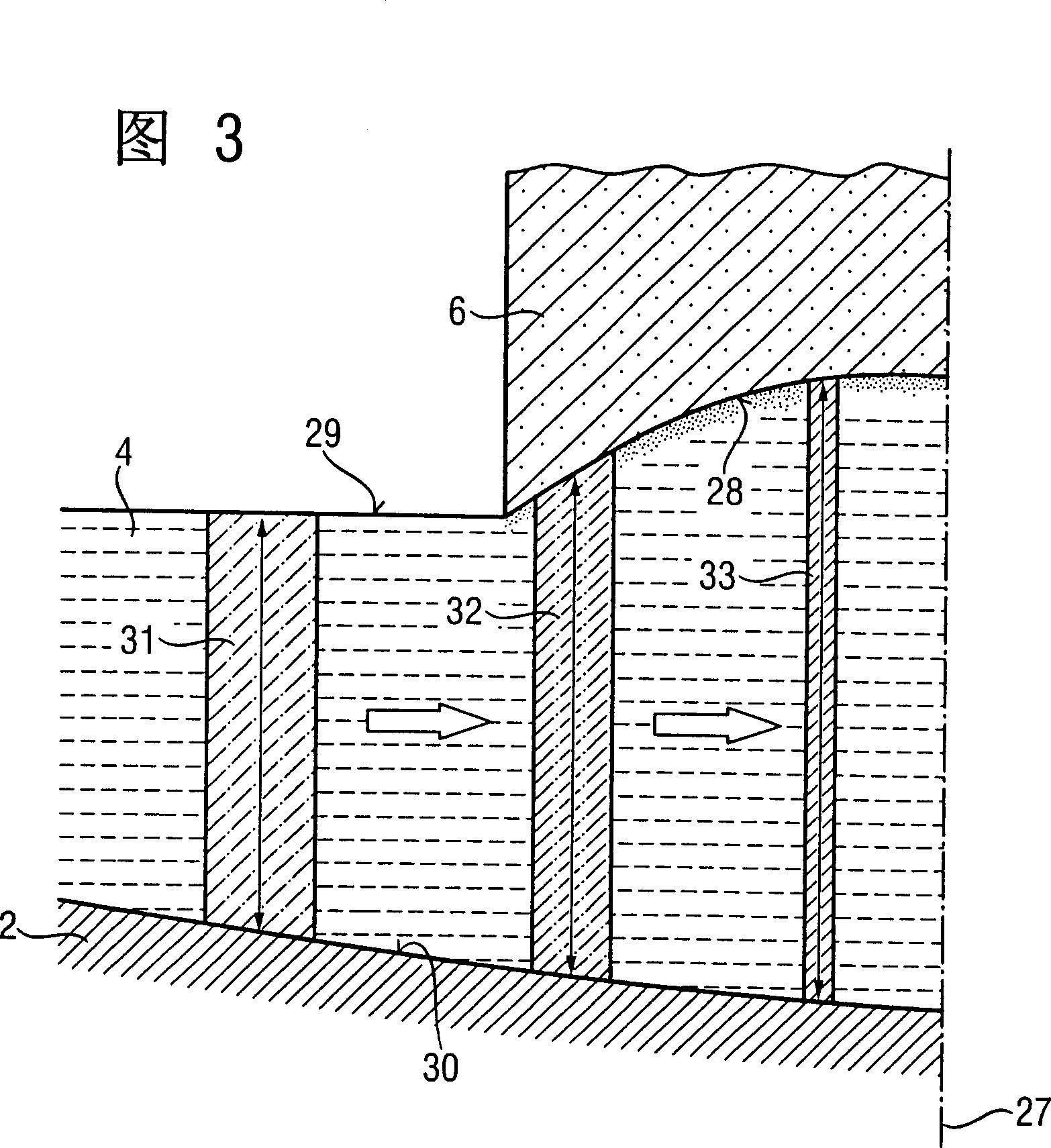
[0080] Fig. 8 shows, when using this crucible to grow a crystal having a diameter of 100mm, along with the profile of the growth interface and the profile of the bottom of the crucible during the growth of the regularly shaped part of the crystal, in the range from the position of the outer wall of the crucible to the position of the central axis The change in the vertical length of the molten liquid layer on the cross-section.

[0081] In Fig. 8, the height is in m...


PUM


Abstract

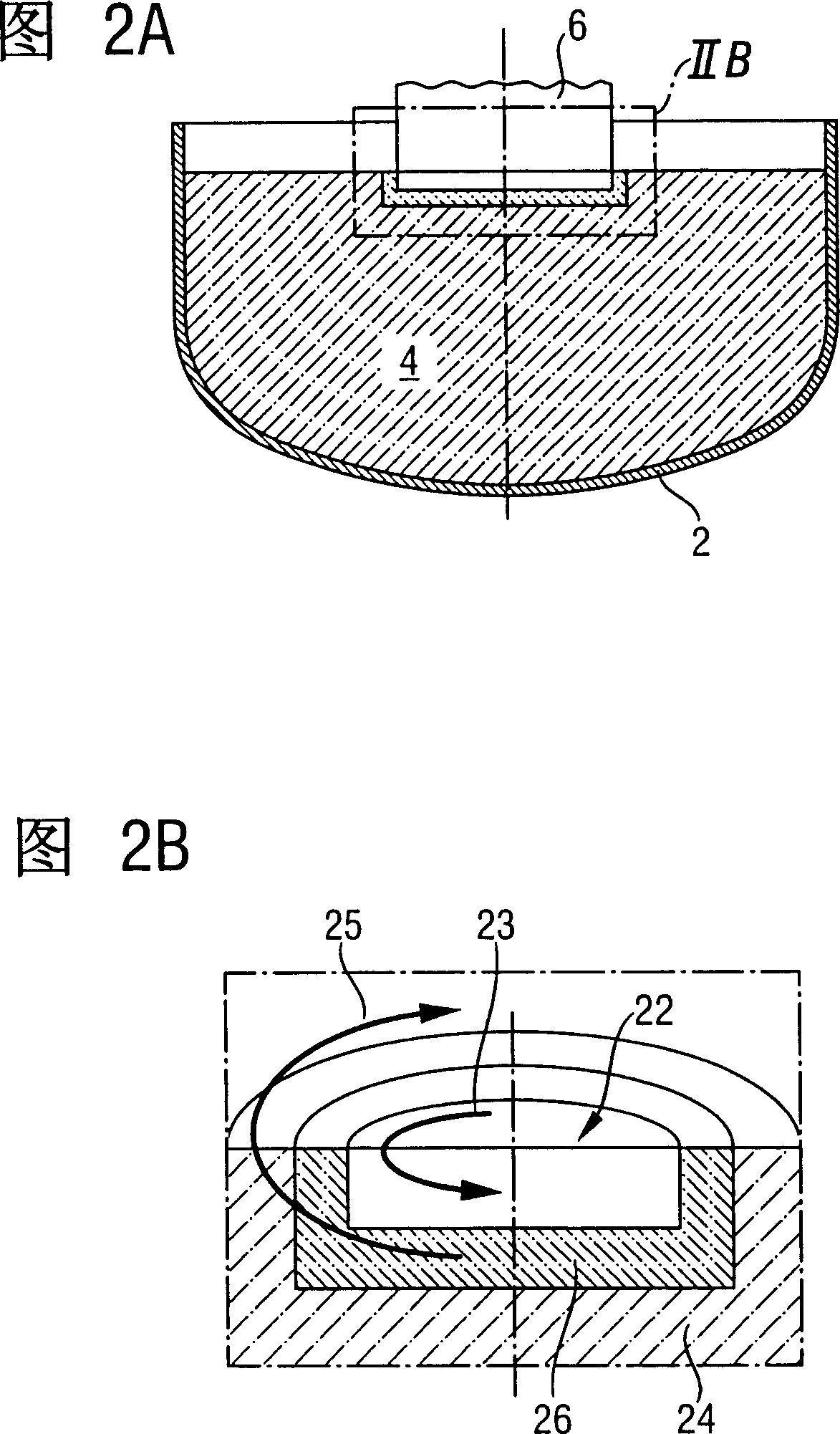
The present invention is to provide a crucible for the growth of silicon crystal, which can enhance the productivity, yield and quality of crystal in the process of silicon crystal growth by Czochralski method, and a silicon crystal growing method by Czochralski method using said crucible. <??>A crucible for the growth of silicon crystal by Czochralski method having an inner bottom surface, the profile of which has at least a raised portion symmetrical about the rotary axis of the crucible wherein the periphery of the raised portion is positioned at a distance of from 0.4 to 1.2 times the radius of crystal to be grown from the rotary axis and the height of the raised portion is from not smaller than 7% to not greater than 100% of the radius of crystal to be grown.

Description

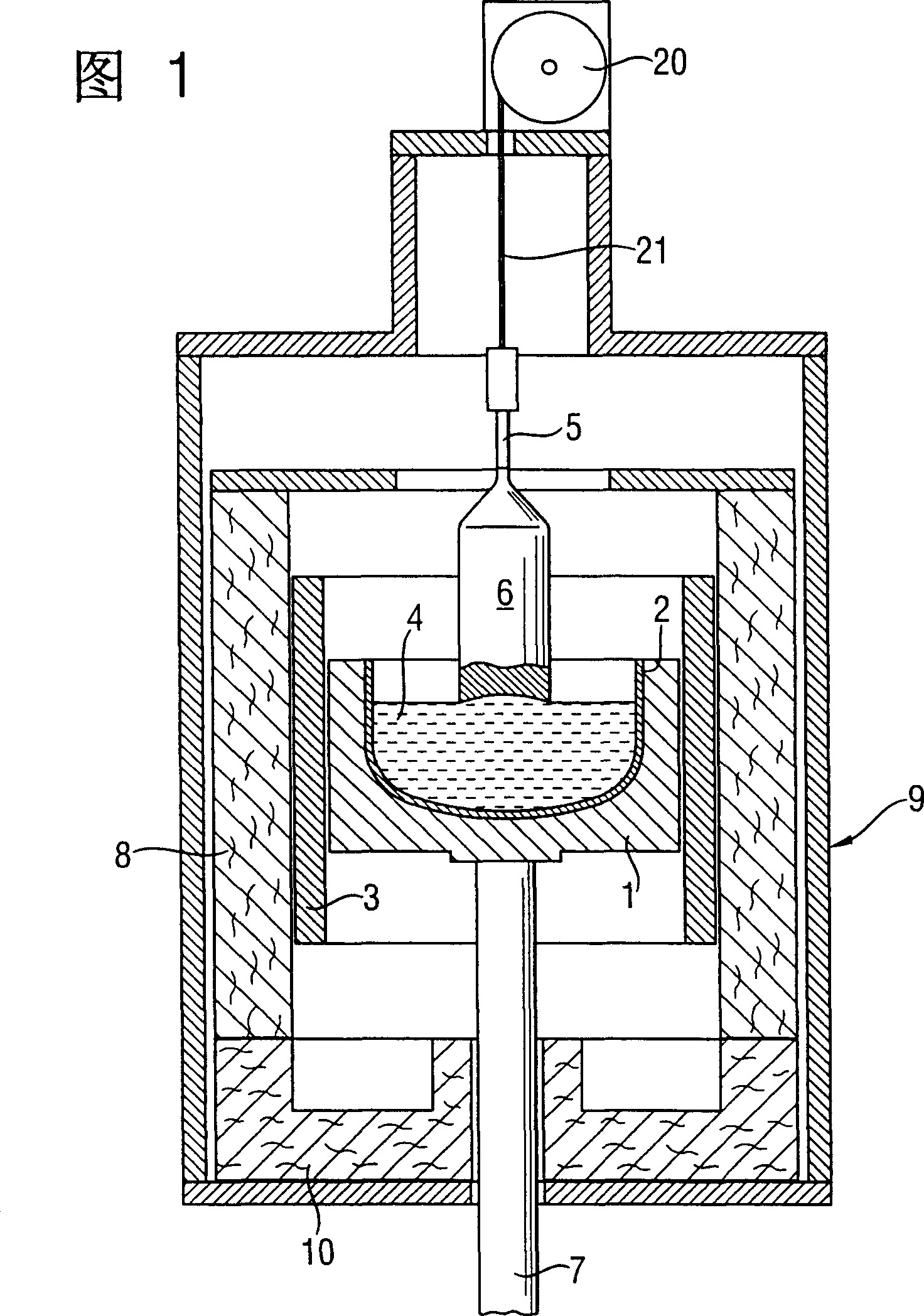
technical field [0001] The present invention relates to a crucible for growing silicon crystals, and a method for growing silicon crystals using the crucible by the Czochralski method, wherein the crucible is used in the method for growing silicon crystals by the Czochralski method Among them, the productivity, throughput and quality of crystals are improved by suppressing deformation of growing crystals. Background technique [0002] Various elemental semiconductor crystals and compound semiconductor crystals have been used as substrates for manufacturing electronic or photovoltaic elements. The Czochralski method (CZ method) has been used as a method for producing these crystals. The CZ method is the most popular method for producing large-sized crystals. Silicon crystals, as the mainstream of semiconductor electronic components today, are mostly produced by the CZ method. [0003] Fig. 1 is a typical longitudinal section of a CZ method crystal manufacturing furnace. I...

Claims


Application Information

Patent Timeline
IPC IPC(8): C30B15/10C30B15/00C30B29/06
CPCC30B15/10Y10S117/90Y10T117/1068Y10T117/10
Inventor 岸田丰玉木辉幸
Owner SILTRONIC AG
Learn More