

Manufacturing method of semiconductor device
A manufacturing method and semiconductor technology, applied in the fields of semiconductor/solid-state device manufacturing, semiconductor device, electric solid-state device, etc., can solve the problems of complicated manufacturing process, position deviation of adhesive film and semiconductor chip, complicated manufacturing process, etc.
- Summary
- Abstract
- Description
- Claims
- Application Information
AI Technical Summary
Problems solved by technology
Method used
Image

Examples
Embodiment approach 1
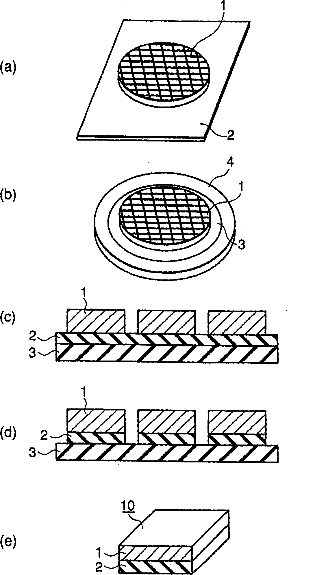
[0059] use figure 1 (a) to (e) describe a method of manufacturing a semiconductor device according to Embodiment 1 of the present invention.
[0060] First, if figure 1 As shown in (a), on a film-shaped adhesive (adhesive film) 2 composed of a mixture of a thermosetting resin mainly composed of polyimide and a thermoplastic resin, a pre-assembled adhesive is bonded at a high temperature by a lamination method. Wafer (single-by-semiconductor chip) 1 divided by dicing. The portion of the wafer 1 to which the wafer 1 is not adhered is then removed. later as figure 1 As shown in (b), the adhesive film surface is laminated and attached to the dicing tape 3 made of, for example, vinyl chloride mounted on the wafer ring 4 at normal temperature. Thus, if figure 1 As shown in (c), the divided wafer (semiconductor chip) 1 is attached to the dicing tape 3 with an equal gap by means of the adhesive film 2 .
[0061] Then, if figure 1 As shown in (d), the adhesive film 2 expose...
Embodiment approach 2
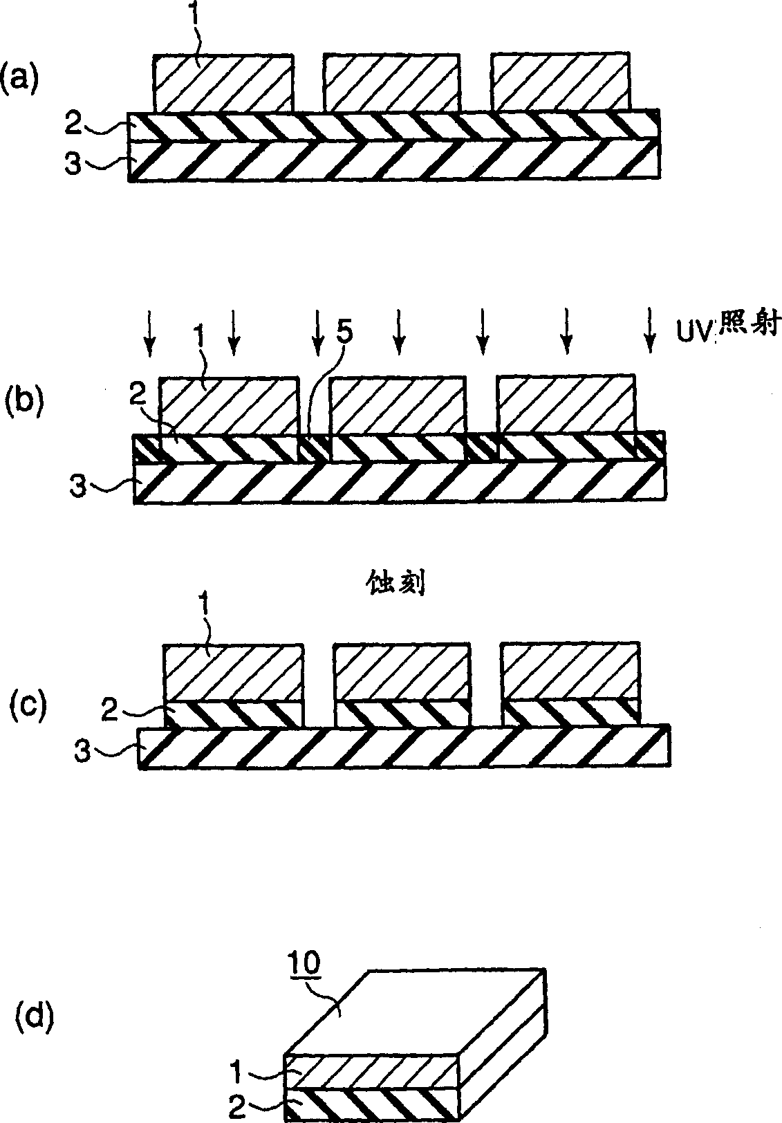
[0066] use figure 1 (a)~(c) and figure 2 (a) to (d) describe a method of manufacturing a semiconductor device according to Embodiment 2 of the present invention.
[0067] Until the structure in which the semiconductor chips 1 are attached at equal intervals on the dicing tape 3 by means of the adhesive film 2 is basically the same as figure 1 Embodiment 1 shown in (a)-(c) is the same. That is, if figure 1 As shown in (a), wafers (semiconductor chips one by one) 1 divided by a pre-dicing method are bonded to a film-like adhesive (adhesive film) 2 by a lamination method or the like at a high temperature. Although the adhesive is a mixture of a polyimide-based thermosetting resin and a thermoplastic resin, in Embodiment 2, the thermoplastic resin has a polymethyl methacrylate structure and contains a compound that is decomposed by UV irradiation. A substance that is a component of a polyreaction.
[0068] The portion of the wafer 1 to which the wafer 1 is not adhered is ...
Embodiment approach 3
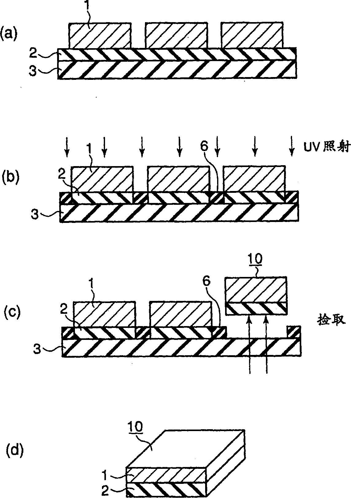
[0074] use figure 1 (a)~(c) and image 3 (a) to (c) illustrate a method of manufacturing a semiconductor device according to Embodiment 3 of the present invention.
[0075] Until the structure in which the semiconductor chips 1 are attached at equal intervals on the dicing tape 3 by means of the adhesive film 2 is basically the same as figure 1 Embodiment 1 shown in (a)-(c) is the same. That is, if figure 1 As shown in (a), wafers (semiconductor chips one by one) 1 divided by a pre-dicing method are bonded to a film-like adhesive (adhesive film) 2 by a lamination method or the like at a high temperature. The agent is a mixture of a polyimide-based thermosetting resin and a thermoplastic resin. In this embodiment 3, as the thermoplastic resin contained in the above-mentioned adhesive film 2, a side chain containing an active ethyl group is used. A substance that undergoes a cross-linking reaction when exposed to irradiation.
[0076] The portion of the wafer 1 to which ...
PUM
 Abstract
Description
Claims
Application Information