Gel structure for combined EMI shielding and thermal control of microelectronic assemblies

A technology of electronic components and conductive gel, applied in the direction of magnetic/electric field shielding, electrical components, electric solid devices, etc., can solve the problem of not completely satisfactorily isolating moisture and dust

Inactive Publication Date: 2002-07-10
TELEFON AB LM ERICSSON (PUBL)
View PDF1 Cites 15 Cited by
  • Summary
  • Abstract
  • Description
  • Claims
  • Application Information

AI Technical Summary

Problems solved by technology

In addition, none of these structures provide a fully satisfactory barrier to moisture and dust, nor provide combined protection of microcircuits from contaminants and vibration and shock while providing EMP shielding and heat dissipation

Method used


Image

  • Gel structure for combined EMI shielding and thermal control of microelectronic assemblies
  • Gel structure for combined EMI shielding and thermal control of microelectronic assemblies
  • Gel structure for combined EMI shielding and thermal control of microelectronic assemblies

Examples


Embodiment Construction

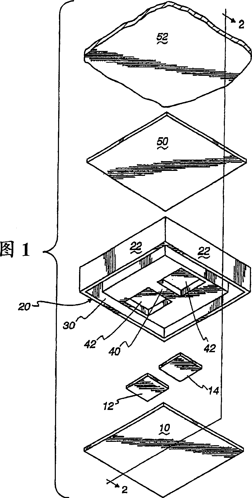
[0021] Figures 1 to 3 show a preferred embodiment of the present invention for use with an electronic assembly that can be used in any electronic device, but is particularly suitable for portable electronic assemblies such as cellular telephones.

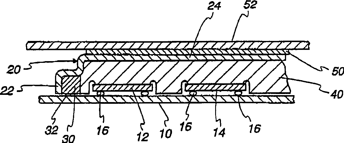
[0022] In the illustrated example, a printed circuit board (PCB) 10 is used to suitably connect suitable microcircuit chips 12, 14, such as flip chips or chip scale packages (CSP). Such as figure 2 As shown, the chips 12, 14 are suitably connected to the printed circuit board 10 by a single mechanical connection 16 in the form of solder balls as shown.

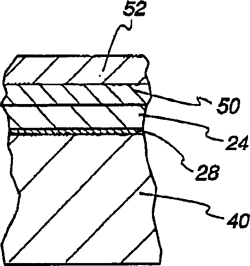
[0023] In the electronic assembly is provided a plastic housing 20 with an outer perimeter 22, one end of the outer perimeter (by figure 2 and 3 The end (defined by the top wall 24 in ) is closed, and the end (the bottom end in the figure) facing the printed circuit board 10 and chips 12, 14 is open. For most applications including, for example, cellular telephones, the plastic h...


PUM


Abstract

A shielding and thermal dissipation structure for an electronic assembly including a distribution circuit and at least one electronic component mounted on a surface of the distribution circuit. A plastic housing overlays the at least one electronic component, and includes an outer periphery defining a housing interior and substantially surrounding the outer periphery of the at least one electronic component. A closed end on one side of the housing outer periphery has an interior surface facing the at least one electronic component with a metal coating about 5 microns thick on the interior surface. The metal coating is chosen from the group of nickel and gold. An electrically conductive gel in the housing interior about the plastic housing outer periphery (and preferably including carbon particles or carbon fibers) is in intimate contact with the distribution circuit and the metal coating. And a thermally conductive gel is disposed between the at least one electronic component and the housing closed end interior surface, and preferable includes particles of at least one of the group of aluminum oxide, aluminum nitride, and boron nitride.

Description

technical field [0001] The present invention relates to an electronic device, and more particularly to the mounting and protection of microelectronic components. Background technique [0002] Electronic devices, especially portable microelectronic devices such as cellular telephones, are required to be used under a variety of conditions that interfere with the proper operation of the device. Vibrations, for example, can rub against contact interfaces inside microelectronic devices. This friction can generate contaminants, such as metal particles, that can migrate within the microelectronic device and degrade the performance of the microelectronic device. In addition, this friction increases the resistance of the contact interface, which also affects the performance of the microelectronic device. Also, shock loads insufficient to cause significant fracture, such as those experienced when the device is dropped, can cause the microelectronic circuitry to lose contact interfac...

Claims


Application Information

Patent Timeline
Patent Type & Authority Applications(China)
IPC IPC(8): H01L23/28H01L23/42H01L23/552H05K7/20H05K9/00
CPCH05K9/0024H01L2224/73253H01L23/42H01L2224/16225H01L23/552H01L2924/00014H05K9/003H01L2224/0401
Inventor 小J·D·麦唐纳德W·M·马钦基维茨
Owner TELEFON AB LM ERICSSON (PUBL)
Why Eureka
Try Eureka