Production method of laminated base material with high integrated level
A manufacturing method and base material technology, applied in the direction of multi-layer circuit manufacturing, layered products, etc., can solve the problems of reducing the layout space of the circuit layer and the inability to effectively improve the circuit integration of the laminated base material.
- Summary
- Abstract
- Description
- Claims
- Application Information
AI Technical Summary
Problems solved by technology
Method used
Image

Examples
no. 1 example
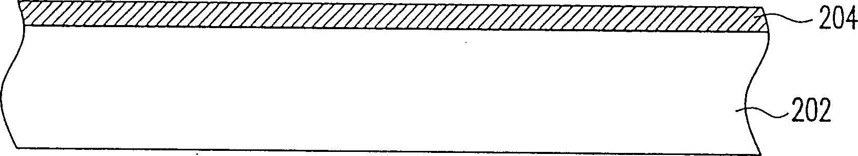
[0028] Figure 2A to Figure 2D It is a schematic cross-sectional view of the manufacturing process of the dielectric layer with patterned circuits in the build-up substrate according to the first embodiment of the present invention. The patterned circuit in the laminated substrate of this embodiment is formed by, for example, metal etching, patterned electroplating, semi-additive method, or full-additive method. In this embodiment, metal etching is used for illustration. First please refer to Figure 2A, providing a supporter 202 , and then forming a conductor layer 204 on the supporter 202 . Wherein, the material of the conductor layer 204 is, for example, copper, and the conductor layer 204 is formed on the support body 202 by, for example, sputtering, pressure bonding or deposition.
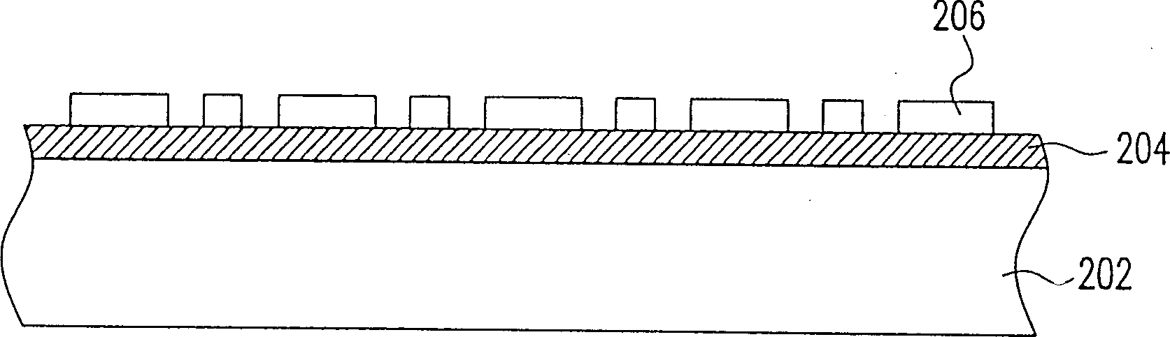
[0029] Then please also refer to Figure 2B and Figure 2C , and then form a patterned photoresist 206 on the conductor layer 204, the patterned photoresist 206 is used to define the patt...
no. 2 example
[0038] This embodiment is the same as the first embodiment in the fabrication of the dielectric layer with via holes and the pad opening layer, but the difference between this embodiment and the first embodiment lies in the dielectric layer with patterned lines way of making.
[0039] Figure 6A to Figure 6D It is a schematic cross-sectional view of the manufacturing process of the dielectric layer with patterned circuits in the build-up substrate according to the second embodiment of the present invention. First please refer to Figure 6A , providing a support body 602 , and then forming a conductor layer 604 on the support body 602 . Wherein, the material of the conductor layer 604 is, for example, copper, and the conductor layer 604 is formed on the support body 602 by, for example, sputtering, pressure bonding or deposition.
[0040] Then please also refer to Figure 6B and Figure 6C , and then forming a patterned photoresist 606 on the conductive layer 604 , the pat...
PUM
 Abstract
Description
Claims
Application Information
 - R&D
- Intellectual Property
- Life Sciences
- Materials
- Tech Scout
- Unparalleled Data Quality
- Higher Quality Content
- 60% Fewer Hallucinations
Browse by: Latest US Patents, China's latest patents, Technical Efficacy Thesaurus, Application Domain, Technology Topic, Popular Technical Reports.
© 2025 PatSnap. All rights reserved.Legal|Privacy policy|Modern Slavery Act Transparency Statement|Sitemap|About US| Contact US: help@patsnap.com