Method for generating blocking metal layer

A metal layer and embolization technology, which is applied in the manufacture of electrical components, electrical solid devices, semiconductor/solid devices, etc., can solve problems such as difficult circuit contact, instability, and high resistance

Inactive Publication Date: 2003-02-19
UNITED MICROELECTRONICS CORP
View PDF0 Cites 13 Cited by
  • Summary
  • Abstract
  • Description
  • Claims
  • Application Information

AI Technical Summary

Problems solved by technology

It is very difficult to make a good circuit contact on a via/contact plug with open porosity, that is, between the irregular uppermost surface of the via/contact plug and the interconnect
Because the metal layer on these irregular surfaces will crack or break after a period of time, and this will cause

Method used


Image

  • Method for generating blocking metal layer
  • Method for generating blocking metal layer
  • Method for generating blocking metal layer

Examples


Embodiment Construction

[0017] The direction of the present invention discussed here is a deposition process of a plug metal layer. In order to provide a thorough understanding of the present invention, detailed steps will be set forth in the following description. Obviously, the practice of the invention is not limited to specific details familiar to those skilled in the art of semiconductor devices. In other instances, well-known process steps have not been described in detail in order not to unnecessarily limit the present invention. The preferred embodiments of the present invention will be described in detail as follows, but in addition to these detailed descriptions, the present invention can also be widely implemented in other embodiments, and the scope of the present invention is not limited, it is subject to the scope of the patent later .

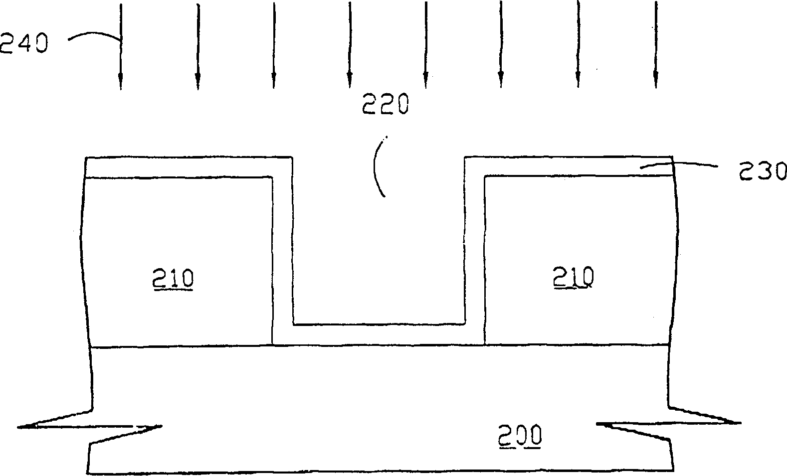
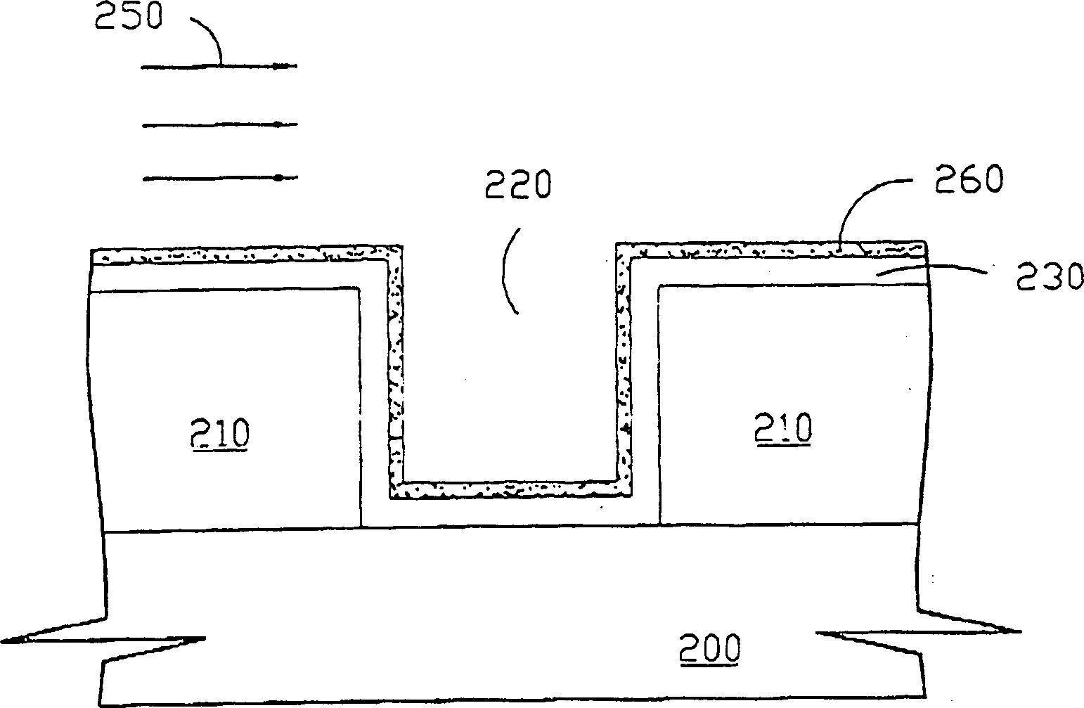
[0018] refer to Figure 2A to Figure 2CAs shown, in the first embodiment of the present invention, a semiconductor substrate 200 having a dielectric ...


PUM

PropertyMeasurementUnit
Thicknessaaaaaaaaaa

Abstract

This invention discloses a new forming method of embollishing metal layers containing providing a semiconductor basic material with a dielectric layer and holes then to form a barrier layer on the side wall of the dielectric layer and the holes and surface of the base to carry on at least one time of ALD to form a (continuous metal seed layer) CMSL on the barrier layer in which ALD steps including filling a mixed gas of hydrogen and silane then cleaning and vacuum, then to inlet metal reacting gas to form a CMSL of 20-40 A and to form a nucleation layer of 20-40 A on the CMSL finally.

Description

(1) Technical field [0001] The invention relates to a method for forming a plug metal layer, in particular to a method for forming a tungsten plug. (2) Background technology [0002] As the density of integrated circuits continues to expand, in order to keep the chip (chip) area the same or even reduce it to continuously reduce the unit cost of the circuit, the only way is to continuously reduce the circuit design specification (design rule) to meet high requirements. The future development trend of the technology industry. With the development of semiconductor technology, the dimensions of components of integrated circuits have been reduced to the deep sub-micron range. As semiconductors continue to shrink down to the deep sub-micron range, some problems arise in process scaling. [0003] The use of titanium nitride layers is well known in the art of manufacturing integrated circuits. The titanium nitride layer is most commonly used as a barrier layer or an adhesion laye...

Claims


Application Information

Patent Timeline
IPC IPC(8): H01L21/285H01L21/768
CPCH01L21/76862H01L21/28562H01L21/76843H01L21/76876H01L21/76846H01L2221/1089
Inventor 王裕标莊佳哲
Owner UNITED MICROELECTRONICS CORP
Why Eureka
Try Eureka