Method for forming integrated circuit with MONOS element and mixed signal circuit

A mixed-signal, integrated circuit technology, applied in the manufacturing of circuits, electrical components, semiconductor/solid-state devices, etc., can solve the complex and difficult problems of single-chip systems, reduce manufacturing process steps, reduce leakage current, and avoid reliability. Effect

Inactive Publication Date: 2003-03-26
MACRONIX INT CO LTD
View PDF0 Cites 2 Cited by
  • Summary
  • Abstract
  • Description
  • Claims
  • Application Information

AI Technical Summary

Problems solved by technology

Also because the manufacturing process used to form logic elements such as metal oxide semiconductor transistors (MOSTransistor) and storage elements such as non-volatile memo

Method used


Image

  • Method for forming integrated circuit with MONOS element and mixed signal circuit
  • Method for forming integrated circuit with MONOS element and mixed signal circuit
  • Method for forming integrated circuit with MONOS element and mixed signal circuit

Examples


Example Embodiment

[0021] It must be noted that the steps and structure of the manufacturing process described below do not include the complete manufacturing process. The present invention can be implemented through various integrated circuit manufacturing process technologies, and only the manufacturing process technologies required to understand the present invention are mentioned here. Hereinafter, a detailed description will be made based on the drawings of the present invention. Please note that the drawings are in simple form and not drawn according to scale, and the sizes are exaggerated to facilitate understanding of the present invention.
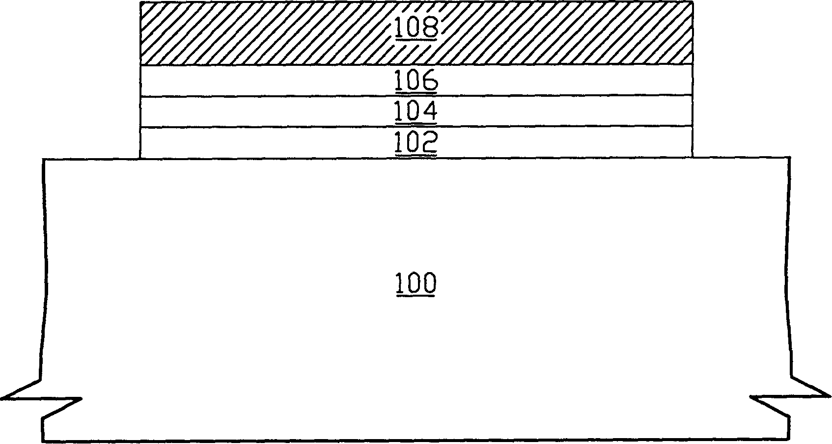
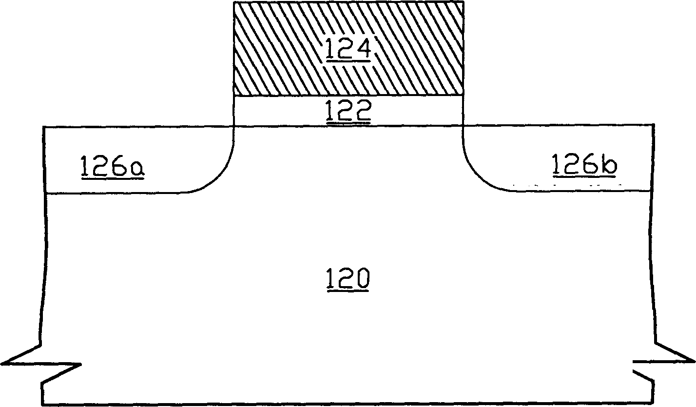
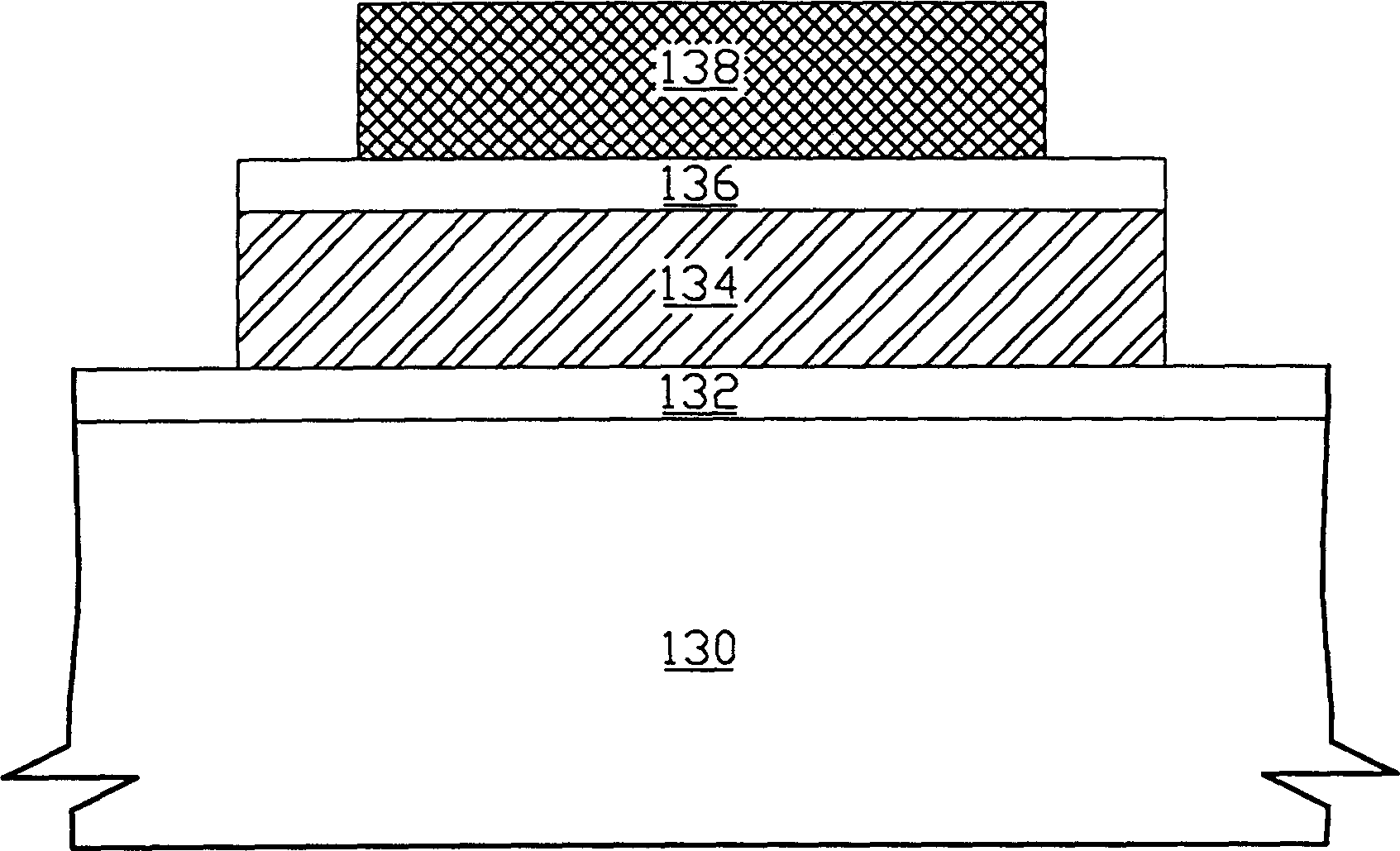
[0022] reference Figure 2A As shown, a substrate 200 is shown. The substrate 200 includes at least an Array Region for forming MONOS storage and a Periphery Region for forming logic elements. The substrate 200 includes at least one silicon substrate with a crystal lattice direction, but is not limited to a silicon substrate with a crystal lattice dir...


PUM


Abstract

The invention relates to a method for forming integrate circuit with and mixed signal, which integrates the non-volatile component such as MONOS storage and logic unit, for example MOS transistor and the PIP capacitor into the single chip of the system by using lesser manufacturing procedure steps.

Description

Field of invention: [0001] The present invention relates to a method for forming integrated circuits, in particular to a method for forming integrated circuits with MONOS (Metal-Oxide Nitride-Oxide Semiconductor) elements and mixed-signal (Mixed-Signal) circuits. Background of the invention: [0002] In view of the ever-increasing demand for integration and diversification of integrated circuits, the industry has widely adopted System on a Chip (SOC) components, which are components with different functions such as logic components and memory Components are integrated into a single chip, and these components are in an interactive relationship with each other. Also because the manufacturing process used to form logic elements such as metal oxide semiconductor transistors (MOSTransistor) and storage elements such as non-volatile memory (Non-Volatile Memory) elements is quite diverse, it is necessary to make logic elements and non-volatile memory elements. SoC of components is...

Claims


Application Information

Patent Timeline
IPC IPC(8): H01L21/82
Inventor 赖二琨陈昕辉陈盈佐黄守伟黄宇萍
Owner MACRONIX INT CO LTD
Why Eureka
Try Eureka