Semiconductor memory
A semiconductor and memory technology, applied in semiconductor devices, static memory, semiconductor/solid-state device manufacturing, etc., can solve problems such as contact hole short circuit and difficulty in ensuring discrete tolerance
- Summary
- Abstract
- Description
- Claims
- Application Information
AI Technical Summary
Problems solved by technology
Method used
Image

Examples
Embodiment 1
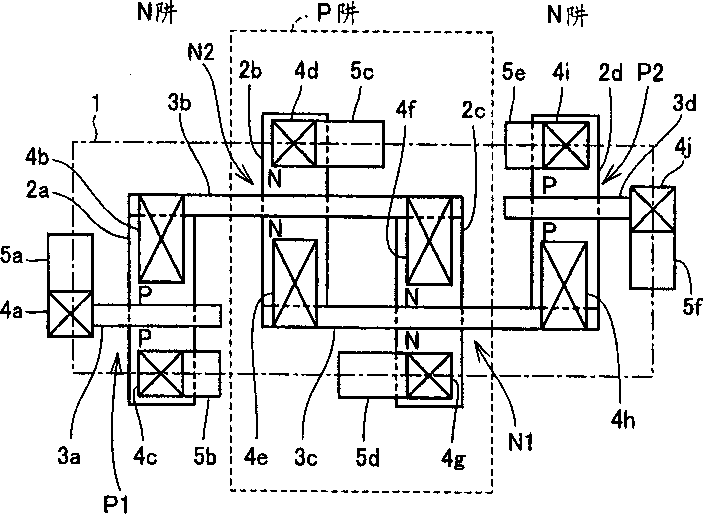
[0070] figure 1 and figure 2 It is a plan view of a memory cell 1 of an unloaded SRAM (static semiconductor memory) in Embodiment 1 of the present invention. exist Figure 19 An equivalent circuit diagram of the memory cell 1 is shown in . again, in figure 1 The layout up to the first metal wiring is shown in the figure 2 The layout of the 2nd and 3rd metal wirings is shown in .
[0071] Such as figure 1 As shown in , the N well region is set on both sides of the P well region. N-type impurities such as phosphorus are selectively implanted into the P-well region to form N-type diffusion regions 2b and 2c, and P-type impurities such as boron are selectively implanted into the N-well region to form P-type diffusion regions 2a and 2d.
[0072]Both the N-type diffusion regions 2b and 2c and the P-type diffusion regions 2a and 2d have linear shapes and extend in the same direction (extending direction of the P well region and the N well region). Thus, the width of the P...
Embodiment 2
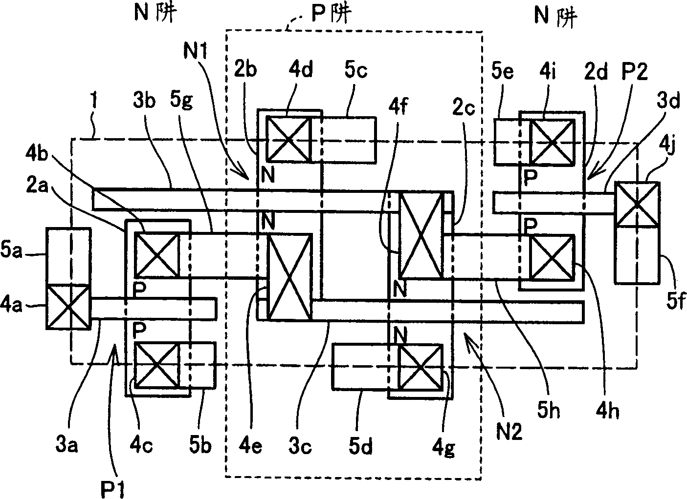
[0093] Second, use image 3 and Figure 4 Example 2 of the present invention will be described. image 3 and Figure 4 is a plan view showing the layout of the SRAM memory cell of the second embodiment. image 3 shows the layout up to the first metal wiring, Figure 4 The layout of the 2nd and 3rd metal wirings is shown in . In addition, the equivalent circuit diagram of this memory cell is the same as that of the first embodiment.
[0094] The main difference from Embodiment 1 is that the drains of the access PMOS transistors P1 and P2 and the drains of the driving NMOS transistors N1 and N2 are directly connected by metal wiring without intervening polysilicon wiring. Specifically, the first metal wiring 5g is used to connect the contact holes 4b and 4e, and the first metal wiring 5h is used to connect the contact holes 4f and 4h.
[0095] Along with this, the positions of the NMOS transistors N1 and N2 are reversed from those of the first embodiment, and the P-type di...
Embodiment 3
[0102] Second, use Figure 5 and Figure 6 Embodiment 3 of the present invention will be described. The third embodiment is an application example of the above-mentioned example. Figure 5 and Figure 6 It is a diagram showing the layout of a 2-port memory cell of an unloaded SRAM cell. Figure 5 shows the layout up to the first metal wiring, Figure 6 The layout of the 2nd and 3rd metal wirings is shown in . exist Figure 20 An equivalent circuit diagram of the memory cell 1 of the third embodiment is shown in .
[0103] In the third embodiment, the important feature is that the third and fourth access PMOS transistors P3 and P4 are added to the memory cell of the second embodiment. Specifically, as Figure 5 As shown in, make the P-type diffusion region 2a in Figure 5 Extended in the up and down direction, polysilicon wiring 3b is formed on the extended part, so that the P-type diffusion region 2d is in the Figure 5 The polysilicon wiring 3f is formed on the exte...
PUM
 Abstract
Description
Claims
Application Information
 - R&D
- Intellectual Property
- Life Sciences
- Materials
- Tech Scout
- Unparalleled Data Quality
- Higher Quality Content
- 60% Fewer Hallucinations
Browse by: Latest US Patents, China's latest patents, Technical Efficacy Thesaurus, Application Domain, Technology Topic, Popular Technical Reports.
© 2025 PatSnap. All rights reserved.Legal|Privacy policy|Modern Slavery Act Transparency Statement|Sitemap|About US| Contact US: help@patsnap.com